
Why Is It So Complicated to Name Chip Process Nodes?
The chip industry often talks about manufacturing nodes, but as Intel's 10nm manufacturing node moves into production, the dialogue among netizens become more and more fierce. The debate over whether TSMC and Samsung have a manufacturing advantage more than Intel is heating up.
Process nodes are usually named after numbers followed by abbreviations for nanometers: 32 nm, 22 nm, 14 nm and so on. There is no fixed and objective relationship between any features of the CPU and the name of the process node. But this is not always the case. From about the 1960s to the end of the 1990s, nodes were named according to the length of their gate lengths. The chart from IEEE shows the following relationship:
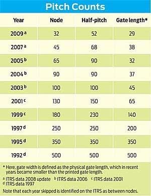
Over a long time, the gate length (the length of the transistor gate) and half pitch (half the distance between two identical characteristics on the chip) matched the process node name, but the last match was in 1997. The half-pitch has always matched the node name in previous generations of CPU, but after that it is no longer relevant. In fact, over a long time, the geometric proportions of processor nodes actually no longer match the ideal evolutionary curve for scaling, as shown in the following picture:
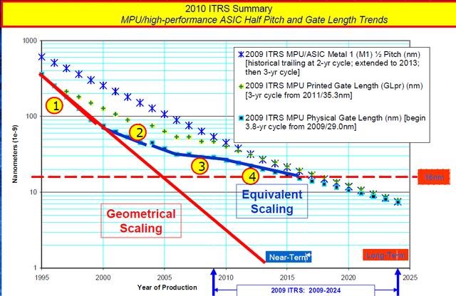
The picture above: the theoretical process node will reach 1 nanometer (red line) in 2015. The blue star represents half pitch and the green star represents grid length.
If we can meet the theoretical requirements to keep the node name and the actual feature size synchronized, then our production process node has dropped below 1nm six years ago.
Now we see that the number used to represent each new node is only the number chosen by the chip company. As early as 2010, ITRS referred to the technique of dumping on each node as "equivalent scaling." As we get closer to the end of the nanoscale, companies may start using the ammeter scale rather than the nanometer scale and in the early days of the chip industry, it was more common to have process nodes in microns rather than nanometers, such as, 0.18 micron or 0.13 micron rather than 180 or 130 nanometers.
How does the market change the rules of nodes
Semiconductor manufacturing involves a large amount of capital expenditure and long-term research. The average time between the introduction of a new technological approach to large-scale commercial manufacturing is about 10-15 years. Few decades ago, the semiconductor industry realized that if a generic node was introduced into the road map and the specific sizes of those nodes, it would benefit everyone in the industry. This will allow all industries needed to bring new nodes to the market to be integrated for extensive and simultaneous development. Over the years, ITRS which is International Semiconductor Technology Road map has released a general road map for the industry. These road maps which lasted for 15 years set overall goals for the semiconductor market.
The picture above: route map, wikipedia image.
ITRS was released in 1998-2015. From 2013 to 2014, ITRS was upgraded to ITRS 2.0, but soon realized its mission scope that is providing future reference for university, associations and industry researchers to stimulate innovation in various fields of semiconductor technology in order to greatly expand its coverage. ITRS has been restructured into a new organization called IRDS that is International Road Map for Equipment and Systems, which has a wider range of tasks and covers a wider range of technologies.
This shift in scope and focus reflects what is happening in the chip manufacturing industry. The reason we stop binding the gate length or half-pitch to the node size is that they either have stopped scaling or have begun to scale slowly. As an alternative, chip companies have integrated various new technologies and manufacturing methods to allow for the continued expansion of nodes. At 40/45 nm, companies like GF and TSMC have introduced immersion lithography. Dual mode was introduced at 32 nm. The gate last manufacturing feature is 28 nanometers. Intel introduced FinFETs at 22nm and 14/16nm nodes and other companies in the industry have introduced FinFETs.
Chip companies sometimes introduce features and functions at different times. AMD and TSMC introduced 40/45 nm immersion lithography technology, but Intel waited until 32 nm to adopt this technology. First, it chose to introduce dual mode. Global chip foundries and TSMC began to adopt a 32/28nm dual mode. TSMC uses a gate structure of 28 nanometers, while Samsung and GF use gate priority technology. However, as the process progress slows down, we see that chip companies pay more attention to marketing, more in the way of defining "nodes" to promote themselves rather than in the physical gate length. Companies like Samsung often introduce digital leading nodes.
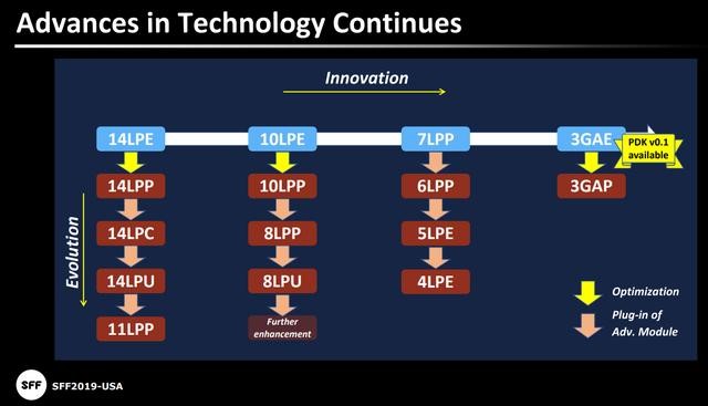
The picture above: Each process node will have room for upgrading, but it is no longer in accordance with Moore's law, that is, what netizen calls toothpaste squeezing.
Although node names are not related to any particular feature size. And, some features have stopped expanding. But, semiconductor manufacturers are still looking for ways to improve key metrics. This is a real engineering improvement. But because today's advantages are hard to achieve and take longer and more expensive to develop. Chip companies are experimenting improvements. For example, Samsung deploys far more node names than before. That's marketing.
Why do people claim that Intel 10nm and TSMC Samsung 7nm are equivalent?
Because the manufacturing parameters of Intel 10nm process are very close to the 7nm process values used by TSMC and Samsung. The following chart is from Wikichips which combines the known functional dimensions of Intel's 10-nm node with those of TSMC and Samsung's 7-nm node. As you can see, they are very similar:
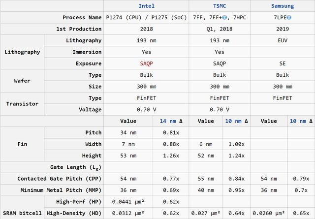
(Image generated by ET, compiled from wikichip data)
You can see from the table that the 14nm/10nm columns show the extent to each company has extended specific functionality down from its previous node. Intel's and Samsung's minimum grid spacing is more important than TSMC's, but TSMC's high-density SRAM point spacing is smaller than Intel's, reflecting TSMC's ability to meet the needs of different customers. Samsung, meanwhile, is even closer than TSMC. Overall, however, Intel's 10nm process node touches many key metrics, but is known as 7nm in both TSMC and Samsung.
Due to specific design goals, single chips still have characteristics that deviate from these dimensions. The information provided by the manufacturer regarding these numbers is an expected implementation of the typical functionality on a given node and does not necessarily exactly match any particular chip.
Some people questioned the difference between Intel's 10nm + process for Icelake and these data that in the table above maybe is Cannon Lake. Admittedly, the expected specifications of Intel 10nm nodes may vary slightly, but 14nm + also changes from 14nm. Intel has indicated that it still sets the 10-nm scale factor at 2.7x rather than 14 nm, so we will postpone any speculation that 10-nm+might be slightly different.

Summary
The best way to understand the meaning of a new process node is to consider it as a general generalization term. When a foundry talks about releasing a new process node, what they say can be concluded into:
"We have created a new manufacturing process with smaller features and stricter tolerances. To achieve this goal, we have integrated new manufacturing technologies. We call this new set of manufacturing technologies process nodes because we need a term that is distinct from the old one and that clearly expresses the concept of progress and improvement capabilities that we have achieved."
Therefore, there are 14nm, 12nm, 11nm, 10nm and 8nm terminology that do not compound the Moore's law but meet the requirements of the industry. The naming of chip process nodes has become complicated and it is still a commercial consideration for chip manufacturers.