
ARM notes: SDRAM memory driver
SDRAM (Synchronous Dynamic Random Access Memory) is also known as memory. Its working principle, control timing, and configuration methods of related controllers have always been difficult in learning and developing embedded systems. Therefore, we analyze the principle from the perspective of its hardware, and then introduce the SDRAM driver’s writing process.
Memory is the execution space of the code. Take the PC as an example. The program stored on the hard disk in the form of a file is loaded into the memory by the operating system before running. Since the memory is RAM (Random Access Memory), the address is used to locate a byte of data. When the CPU executes the program, the value of the PC is set to the start address of the program in the memory. The CPU will sequentially fetch, decode and execute the address from the memory. Before being initialized, memory, like an unbuilt house, can't read and store data. Thus, we must initialize the memory if MTOS is running in memory.
Universal storage device:
Before introducing the working principle, it is necessary to understand the storage mode of the storage device: ROM, RAM
ROM (Read-Only Memory) is a solid-state semiconductor memory that can only read pre-stored data. Once the data is stored, it can no longer be changed or deleted. It’s usually used in electronic or computer systems such as BIOS in PC that do not require frequent changes to the data. The data will not disappear although the power is turned off.
RAM (Random Access Memory) is a memory where the contents of the storage unit can be freely withdrawn or deposited on demand, and the access speed is independent of the location of the storage unit. That’s to say, when you give a random and valid access address, RAM will return its stored content (random addressing), and its access speed is independent of the address. Because it will lose its stored content during power failure, RAM is mainly used to store programs for random access in a short time. The memory address in a 32-bit computer system is a four-byte aligned address. The fetch, execution and storage of CPU are through the address, so it can be used as memory.
RAM is divided into DRAM (Dynamic RAM) and SRAM (Static RAM) according to different hardware.
The basic original of DRAM is a small capacitor which can retain the charge on two plates for a short time, and represent the 0 and 1 in the computer through the voltage difference between the two poles. The capacitor should be periodically charged, otherwise the data will be lost. The charging process is called refresh. Thanks to the simple manufacturing process, small size, and easy to be integrated, capacitor is often used as the original memory in the computer such as the memory of PC, SDRAM, DDR, DDR2, DDR3, etc. However, it is a disadvantage: the access speed is slower due to the need to periodically refresh the storage medium.
SRAM is a memory with static access function, which can save the data stored in it without refreshing the circuit, as a result of fast access speed. But its large size, large power consumption, and high cost makes it used in applications where the storage capacity is not high but the access speed is fast, such as the CPU L1 cache, L2 cache (level 1 and level 2 cache), register.
The MINI2440 is shipped with three storage media at the factory to meet the needs of development:
(1) NOR FLASH (2M): ROM is usually used to save BootLoader and boot system boot.
(2) NAND FLASH (256M): The model is different, Nandflash is different in sizes. Nandflash is used to save operating system image files and file systems.
(3) SDRAM (64M): A memory is used to executive program.
NORFLASH: It supports for XIP (eXecute In Place) so that applications can run directly in Flash without having to read the code into system RAM, which means random addressing. The cost of NOR FLASH is high.
NAND FLASH: It provides extremely high cell density leading to high storage density, and fast writing and erasing speeds. Its cost is low but XIP is not supported. It can be used as a data storage medium in the embedded system such as mobile phone memory card, SD card, etc.
1.1.1 S3C2440 Memory Address Segment (Bank)
S3C2440 externally leads to 27 address lines ADDR0~ADDR26, which can address up to 128MB, while it can reach 1GB. This is because S3C2440 divides 1GB address space into 8 BANKS (Bank0~Bank7), each of which corresponds to a chip-selected signal line nGCS0~nGCS7. When accessing BANKx, the nGCSx pin level is pulled low to select an external device. The S3C2440 can be accessed up to 1GB through 8 signal lines and 27 address lines. As shown in Figure 2-48.
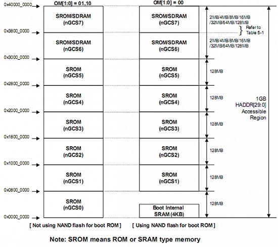
Figure 2-48 S3C2440 memory BANK
As is shown in the figure, the picture on the left corresponds to the memory Bank distribution map when the Nandflash is not used (set by jumper). Norflash is usually selected to start in this startup mode, and it is soldered to Bank0. After the system is powered on, the CPU starts to fetch and run from Bank0 start address 0x00000000.
The picture on the right introduces the boot from Nandflash (set by jumper). After the system is powered on, the CPU will automatically copy the first 4K data in Nandflash to a 4K SRAM memory inside S3C2440 (called Steppingstone), and then fetches the address from Steppingstone.
Bank0~Bank5 can solder ROM or SRAM type memory, while Bank6~Bank7 can solder ROM, SRAM and SDRAM. That is to say, S3C2440 SDRAM should be soldered on Bank6~Bank7, maximum support 256M. Bank0~Bank5 usually solder small-capacity ROM booting the system. What kind of memory and how much capacity is soldered depending on the manufacturer of each development board. For example, the MINI2440 development board solders 2M Norflash to Bank0 for storage system booting program bootloader. Two piece of 32M SDRAM with the width of 16 bit are soldered on Bank6 and Bank7, forming a 64M and 32-bit memory in parallel.
Since the S3C2440 is a 32-bit chip, theoretically it can reach the 4GB addressing range. Except for the above 8 BANKs for connecting external devices, some of the address space is used for registers with special function, and the rest are not used.
Table 2-14 address space of S3C2440 device register