
Break through process:Why is 7nm the physical limit?What is the 1 nm manufacturing process in America?

Moore's Law, which has been applied for more than 20 years, has gradually shown signs of failure in recent years. From the perspective of chip manufacturing, 7nm is the physical limit of silicon chips. However, foreign media reported that a team at Lawrence Berkeley National Laboratory broke the physical limit by using carbon nanotube composites to reduce the most sophisticated transistor process from 14nm to 1nm. So, why is 7nm the physical limit of silicon chips? What are the carbon nanotube composite materials? What should China do in the face of technological breakthroughs in the United States.
What is the XX nm manufacturing process?
The manufacturing process of chip is often expressed as 90nm, 65nm, 40nm, 28nm, 22nm and 14nm, for instance, Intel's latest six-generation Core series CPU adopts its own 14nm manufacturing process. Hundreds of millions of transistors, consisting of a source, a drain, and a gate between them, are integrated into the current CPU, with the current flowing from the source to the drain, and the gate controlling the current.
The so-called XX nm actually refers to the gate width of the complementary oxide metal-semiconductor field-effect transistor formed on the CPU, also known as the gate length.
The shorter the gate length, the more transistors can be integrated into silicon wafer with the same size– Intel once claimed that when reducing the gate length from 130nm to 90nm, the size of transistors will be reduced by half; In the case of similar integration of chip transistor, the more advanced manufacturing processes, the smaller the chip area and power consumption, the lower the cost.
The gate length can be divided into an actual gate length and a lithography gate length determined by lithography technology. Due to the diffraction phenomenon in lithography and the process of ion implantation, etching, plasma washing, heat treatment, etc. in chip manufacturing, the lithography gate length may be inconsistent with the actual. Even under the same process, the actual gate length will be different too. For example, although Samsung also introduced a 14nm process chip, there is a certain distinction exiting in the actual gate length of the 14nm chip between Samsung and Intel.
Why is 7nm the physical limit?
It was previously explained that shortening the length of the transistor gate allows the CPU to integrate more transistors or to effectively reduce the transistor area and power consumption, as well as cutting the silicon cost of the CPU. As a result, CPU manufacturers have spared no effort to reduce the transistor gate width to increase the number of transistors integrated per unit area. However, this method will shorten the distance of electron movement, which easily causes the electrons in the transistor to spontaneously flow from the negative pole to the positive pole through the silicon substrate of the transistor channel, that is, leakage. Moreover, as the number of transistors in the chip increases, the silicon dioxide insulating layer, which is originally only a few atomic layers thick, becomes thinner and leads to leakage of more electrons, in turn the leakage current increasing the additional power consumption of the chip.
In order to solve the problem of leakage, Intel, IBM and other companies have gone to great lengths. Intel has integrated high-dielectric thin film and metal gate integrated circuits in its manufacturing process; IBM developed SOI technology - a strong dielectric film is buried in the source and drain; In addition, there is fin-type field-effect transistor technology , which increases the capacitance value by increasing the surface area of the insulating layer, and reduces leakage current to prevent electronic transitions.
The above method can effectively solve the problem of leakage to a certain extent when the gate length is longer than 7 nm. However, on the basis of the existing chip materials, once the transistor gate length is shorter than 7 nm, a tunneling effect of electrons in transistor is easy to occur, which poses a huge challenge for chip manufacturing. In response to this problem, it’s an effective way to find new materials to replace silicon to make transistors below 7nm.
1nm process transistor is still in the laboratory stage.
Carbon nanotubes(CNTs) are related to grapheme, which is very popular in recent years. Zero-dimensional fullerene, one-dimensional carbon nanotubes and two-dimensional graphene all belong to the family of carbon nanomaterials, and they can be transformed in form if certain conditions are satisfied. CNT is a kind of one-dimensional material with a special structure with a radial dimension of nanometer and an axial dimension of micron. The tube is generally sealed at both ends, so it has great strength, and the large aspect ratio is expected to make it an extremely tough carbon fiber.
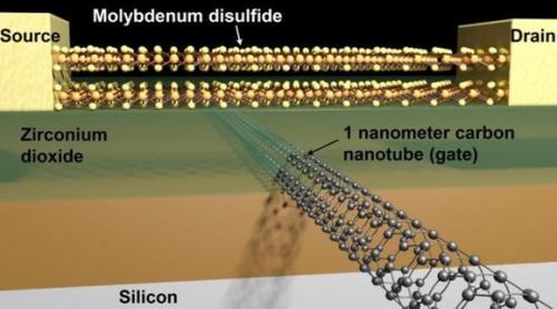
Carbon nanotubes and graphene have similar properties in electricity and mechanics. Thanks to better electrical conductivity, mechanical properties and thermal conductivity, carbon nanotube composite materials have a good application prospects in supercapacitors, solar cells, displays, biological detection, fuel cell and so on. In addition, carbon nanotube composite materials doped with some modifiers have also attracted much attention. For example, CdTe quantum dots are added to a graphene/carbon nanotube composite electrode to make photoelectric switches, and metal particle is doped to fabricate a field emission device. The foreign media reported that Lawrence Berkeley National Laboratory has reduced the most sophisticated transistor process from 14nm to 1nm, whose transistors are made of carbon nanotubes doped with molybdenum disulfide. However, this technology is only at the stage of technological breakthroughs in the laboratory, and there is currently no commercial mass production capability. It remains to be seen whether the technology will become mainstream commercial technology in the future.
Technological advances do not necessarily bring commercial benefits
Over the past few decades, China's semiconductor manufacturing technology has been pulled a long way from catching up with the West because Moore's Law has really worked. In recent years, the slow progress of chip manufacturing technology and the failure of Moore's Law have been a great advantage for Chinese semiconductor industry to catch up with the West. There are two reasons for the failure of Moore's law. On the one hand, there are technical factors – huge difficulty in research and development technology of advanced lithography machines, etching machines and other equipment, as well as advanced chip manufacturing technology, and high capital requirements. On the other hand, there are commercial factors.
Every advancement in the manufacturing process can lead to huge profits for chipmakers before the manufacturing process reaches 28nm. However, advances in manufacturing at 14/16nm can actually increase the cost of the chip--when Intel first developed the 14nm manufacturing process, it was reported that its mask cost was $300 million. Of course, as time goes by, TSMC and Samsung master the 14/16nm process so that the price isn’t so expensive now. But Intel is working on a 10nm process that would cost at least $1 billion, according to Intel's official estimates. The reason why new manufacturing process is expensive is not only the high development cost and low yield of the new process, but also the extremely expensive equipments such as lithography machines and etching machines. Therefore, even if the advanced manufacturing process is technically mature, customers will hesitate to adopt the most advanced manufacturing process due to the too high mask cost. For example, if the output of the 10nm process chip is less than 1000 million, the cost of masking on each chip is as high as $100. The international general low-profit chip design company’s pricing strategy is 8:20 pricing method ,that is, the hardware cost is 8 while priced at 20. Don't think this price is high, in fact very low. Intel's general pricing strategy is 8:35. What’s more, AMD has reached 8:50 in history. In short, the price of a 10nm CPU will not be less than $250, even excluding the cost of produce, package and test. At the same time, relatively few customers can make it difficult to share huge costs