
Can compare with the 7nm differentiation scheme? Global Foundry launches 12LP+ process
Can compare with the 7nm differentiation scheme? Global Foundry launches 12LP+ process
Under the special circumstances of last year, the chip industry has made great improvements. However, the rapid changes in the industry have even made it difficult for international chip giants to adapt and adjust their strategic plans in order to achieve more stable development. Global Foundry, which is the world's second-largest pure-film foundry company, has already announced the abandonment of its 7nm chip production project last year, and focus on producing 12nm chips that can meet with most market needs.

Why does the Global Foundry give up the 7nm and switch to produce 3D package?
1. 3D package technology has become the main development priority of semiconductor giant
Intel and TSMC, both of which are semiconductor giants, are investing earlier and more in 3D packaging than Global Foundry. At the end of last year, Intel launched the world's first 3D packaging technology, Foveros, on its "Architecture Day". At the CES2019 exhibition held shortly thereafter, the Lakefield chip packaged with Foveros technology was exhibited. According to Intel, the biggest feature of this technology is that it can stack another logic chip vertically on the logic chip, realizing the true 3D stack.
At the SEMICON West conference held recently, Intel once again launched a new packaging technology Co-EMIB. It enables the interconnection of two or more Foveros components and essentially achieves the performance level of a single chip. Designers can also use Co-EMIB technology to achieve high bandwidth and low power connection simulators, memory and other modules.
TSMC has also invested in 3D packaging for a long time. There is a saying in the industry that it is because of TSMC's emphasis on advanced packaging technology that enabled it to gain an advantage in competition with Samsung and received orders from Apple. Regardless of whether this statement is true or not, the importance of packaging technology in TSMC's technical layout has become increasingly prominent.

2. The package subsystem "IP" may become one of the trends
As the demand continues to increase, if all the circuits are integrated on one chip, the chip area will be too large, the design cost and process complexity will be increased, and the product cycle will be prolonged, thus increasing the complexity of the manufacturing process and manufacturing costs. This is also the main challenge people are facing in the era of heterogeneous computing. Therefore, from the perspective of technology trends, mainstream semiconductor companies rely on 3D packaging technology to implement the complex system level chips.
People are also exploring the way to decompose a complex chip into several subsystems multi-chip by using heterogeneous integration method, some of the subsystems can be standardized and then packaged together like an IP core. This may be a development direction for future chip manufacturing. Of course, at present, this method is not without obstacles. The first thing to solve is the heat dissipation problem.
The focus of the Global Foundry after the "slimming"
Since January of this year, Global Foundry has sold several fabs and related businesses.
Due to the huge capital required to invest in the advanced processes, Global Foundry announced that it would suspend the development of 7nm process technology and put more energy into the more matured technology. According to relevant data, TSMC's market share in the second quarter of 2019 was 49.2%, followed by Samsung (18.0%), Global Foundry (8.7%), UMC (7.5%) and SMIC (5.1%). The market share of Global Foundry fell from the original second position to the third place, and was more than doubled by Samsung. At the same time, the gap between Global Foundry and TSMC is getting larger and larger.
However, Global Foundry also has its own plans, it gradually focusing on the Internet of Things (IoT) and radio frequency (RF) technology.
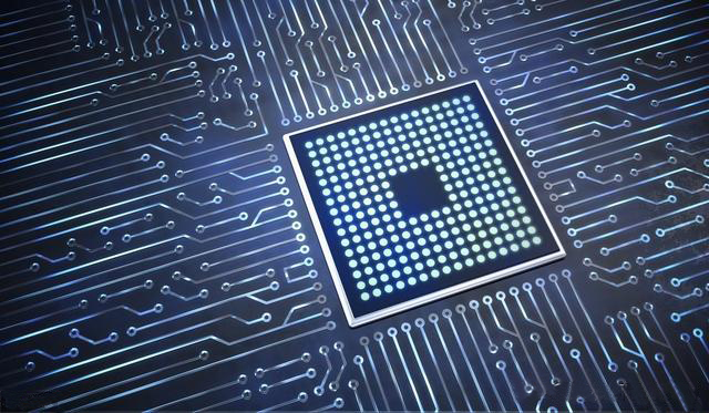
Global Foundry launches 12LP+ process
On September 25th, Global Foundry launched the 12LP+ process at its global technology conference, it mainly focus on artificial intelligence training and reasoning applications. Compared to the previous 12LP process generation, the 12LP+ offers a 20% performance increase or a 40% power reduction with a 15% reduction in logic area.
In addition, a key feature of the 12LP+ process is the high-speed, low-power 0.5V SRAM memory cell that supports fast, energy-efficient data transfer between the processor and memory. This is an important requirement for smart applications by the computing and wireline infrastructure market.
Global Foundry provides design reference packages for artificial intelligence applications and design/technical joint development (DTCO) services for the 12LP+ process, both of the services allow customers to view artificial intelligence circuit designs from a holistic perspective in order to reduce energy consumption and cost.
In addition, 12LP+ also has a new silicon interposer for 2.5D packaging, which helps integrate high-bandwidth memory with the processor for fast, energy-efficient data processing.
Gus Yeung, general manager and researcher at the Physical Design Group in ARM, said: "Artificial intelligence, automotive and high-end consumer mobile are just a few of the growing applications to meet with the urgent needs of high-performance SoCs. Supported by the widely used ARM Artisan physical IP and advanced processor design, the Global Foundry 12LP+ will help designers design products faster and more efficiently."
Michael Mendicino, vice president of digital technology solutions at Global Foundry, said: "The launch of 12LP+ is the result of Global Foundry's strategy of providing differentiated solutions for customers. Compared with other solutions, Global Foundry can expand the design scale without interrupting the workflow. This is very cost effective."
Michael Mendicino further stated: “For example, as an advanced 12nm technology, our 12LP+ solution has provided customers with most of the performance and power advantages they want from the 7nm process, but the average cost of their NRE (non-repetitive engineering) is only about half, which brings significant cost reduction. In addition, because the 12nm node runs longer and is more mature, customers will be able to quickly streamline to fully grasp the growing demand for artificial intelligence technology. ”
According to Global Foundry, 12LP+PDK is now available and the company is currently working with several customers. It is expected to be released in the second half of 2020 and mass production will start in its Fab 8 in Malta, New York in 2021.