
Do you know any other misconceptions about embedded flash memory?
The development and innovation of the automotive industry has been driving the development of semiconductor industry over the years. According to IHS data, the annual revenue of the automotive semiconductor market has exceeded $30 billion, and will continue to rise with the increase of ADAS, fuel efficiency and convenience. At present, the total value of semiconductor components in each luxury car is about $1000, while that in mid-range car is about $350. MCU is an important part of automotive. Most automotive MCUs have on-chip embedded flash memory, which contains complex and detailed instruction codes. Although embedded flash memory as a model for non-volatile memory technology based on polysilicon floating gate is widely deployed in a series of products in automotive, industrial and consumer applications, there are still some misconceptions about embedded flash technology, which is what I want to clarify.
Embedded flash solutions save time and money.
Most of the time, the higher is the price, the better is the quality. Polysilicon floating-gate embedded flash solutions seem to be more expensive than charge trap-based solutions like SONOS. Because polysilicon floating-gate embedded flash typically requires more shielding steps than embedded non-volatile memory solutions based on charge traps. However, chip designers should carefully consider the total cost of non-volatile solutions, including potential production losses, losses due to on-site rebates, long-term data retention, total chip size including ECC and required redundant circuits, and production time. In addition, charge trap-based solutions are not suitable for high-temperature and high-durability applications. So if non-volatile memory platforms need to meet the needs of a range of low-end and high-end applications, there is a greater need for non-volatile memory solutions that meet all application requirements, such as voltage, operating temperature, data retention and durability. Applying multiple non-volatile platforms to a technology node is much more expensive than polysilicon floating-gate.
Differentiated polysilicon floating-gate embedded flash memory
Over the years, most IDMs have used similar 1T polysilicon floating-gate stacking solutions for applications that require embedded flash memory. In the past two decades, the innovative segregated floating-gate Superflash Technology continues to drive the industry forward with its differentiated and efficient polycrystalline sillicon erasure and source injection programmable storge units.
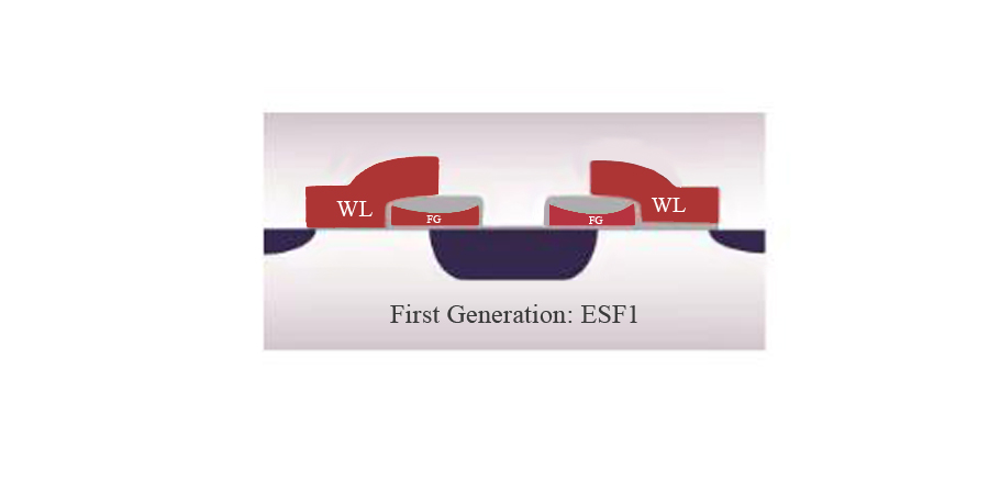
Figure 1 The first-generation embedded SuperFlash(ESF1)
Here we will show the basic bit unit storage structure and working principle of flash memory. See the following three pictures.
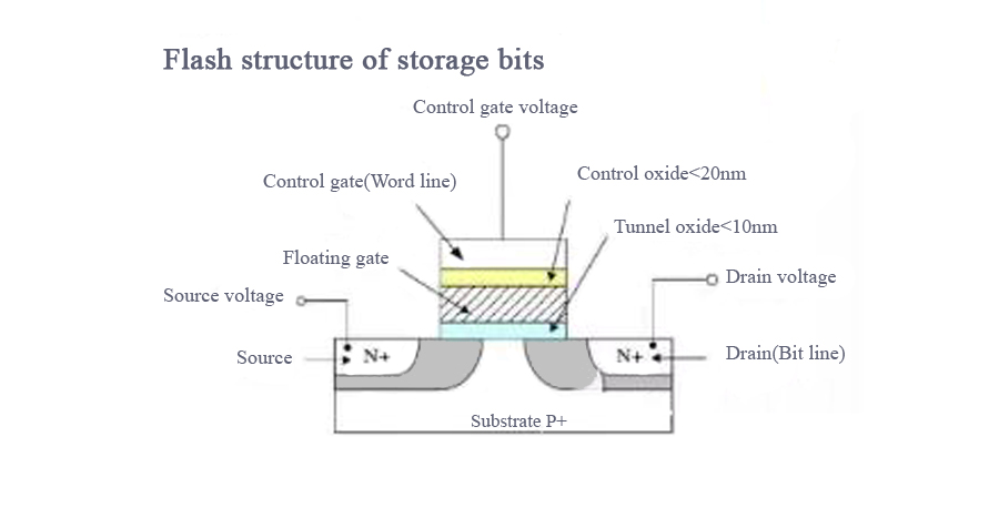
Flash structure of storage bits
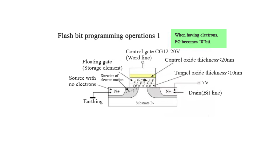
Flash bit programming operations 1
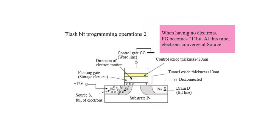
bit programming operations 2
The low operating voltage of embedded flash memory make it ideal for IoT applications
IoT applications require low-voltage read/write operations. Even if the programming/erasuring operation requires a high voltage, the process is transparent to the user because the macro flash receives the core/IO voltage from the user and uses an internal charge pump to raise it to the high voltage required for programming and erasuring operations. As a result, embedded flash can be immediately used in low-power IoT applications.
Embedded flash memory supports EEPROM function.
Traditional EEPROM architecture supports byte of write operations, often used by applications that need to update data frequently. Typically, embedded flash memory is a set of storage units arranged according to certain rules, also known as sectors. Sectors need to be completely erased before writing new data. Fortunately, we can use SRAM buffer to simulate EEPROM function on a small portion of the entire embedded flash memory area, which is simple and transparent to the user.
This often makes people misunderstand that embedded flash memory does not meet the requirements of EEPROM durability. However, EEPROM can usually be rubbed up to 1 million times. In the past, the number of erasure required by most MCU and smart card applications is less than 100,000, but recent applications such as SIM cards are required to be rubbed up to 500,000 times (typical values). To meet this requirement, we offer better erasure resistance through the third generation of SuperFlash technology (ESF3) which is better than the previous two generations. A large amount of data shows that third-generation technology can meet the rubbing requirements of 500,000 times.
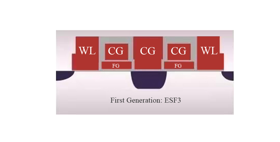
Figure 2 The third-generation embedded SuperFlash(ESF3)
Embedded flash memory can be extended
Ten years ago, many people thought that embedded flash memory cannot break through the nodes below 90nm. The reason was that the expansion of storage unit faced many difficulties and challenges. But now embedded flash memory has developed to 28nm, which proves it was a wrong view. The challenge now is to move embedded flash into the FinFET process era. However, foundries such as Samsung and GLOBALFOUNDRIES are focusing on FDSOI technology for planar 22-nm technology nodes (or even smaller), which may make embedded flash memory longer service life than a 28-nm nodes.
For instruction code applications, OTP cannot replace embedded flash memory.
Some integrated circuits require on-chip instruction codes for one-time programming, which can be done on site or at final testing after wafer-level testing or encapsulation is completed before delivery to the customer. Although OTP solution appears to be sufficient to meet the one-time programming requirements for non-volatile memory, there are some serious user experience and reliability issues in its actual operation. First of all, the OTP programming of large storage blocks requires the use of multiple redundant bits and related redundant management circuits, and there are difficult inefficiencies to solve. Additional complexity also makes chip designers nervous. Second, embedded flash process is optimized for long-term data reliability. Compared with this, the data retention time provided by large storage blocks with OTP solutions usually has no advantage. The reason is that there are some uncertainties in programming large OTP storage blocks, and the resulting tail will affect the accurate reading.
Embedded flash memory is scalable and can be used in advanced technology nodes of OEM plants.
Typically, embedded flash memory is two generations later than the leading technology nodes, because it is driven primarily by the requirements of non-volatile memory solutions. However, advanced nodes such as 14nm FinFET are driven by high-end SoC, high-performance computing, and graphics processors, which do not require on-chip embedded flash memory. Recently, there has been a big step in the availability of advanced logical nodes for embedded flash. Only 90 nm embedded flash memory was available in pure foundry plants in 2012. But over the past four years, embedded flash memory has reached 28nm in many of the leading foundry plants (see Figure 1) and in the development of high-end automotive and IoT solutions. This leap-forward development is mainly driven by automotive applications, which require the use of automotive MCU for advanced technology nodes.
Automotive, mobile and IoT applications are driving the development of single-chip computer and other flash devices, contributing to flash market increasing to around $22 billion. In order to occupy a place in this market segment, many foundry plants have launched or are actively working on embedded flash platforms, including GLOBALFOUNDRIES、HHGrace、LFoundry、SilTerra、TSMC、UMC、Vanguard XFAB and XMC. More members will join in the future.
All IDMs without wafer factories or many IDMs with small wafer factories are cooperating with pure foundry plants. However, IDMs have their own manufacturing equipment so they can either produce flash by themselves or outsource flash to pure foundry plants, according to the product set and available technology. Many first-class IDM