
Efficient power supply methods for SD flash memory of smart phone
The demand for storage functions of mobile phone is growing rapidly. In this paper, the development of memory and several different power supply methods of SD flash are discussed.
The ability to capture, display, and share video and image content drives the growing demand for memory. Capture functions are rapidly improving thanks to the advent of small camera optics, highly integrated image processing, and advanced flash technology (using brighter LED solutions and smaller xenon light solutions). Thin and efficient touchscreen LCD, AMOLED and Ultra-AMOLED solutions, combined with an intuitive and convenient user interface, make the display of images and video images simple and vivid. In addition, ubiquitous network connectivity, various social networks, and the presence of a large number of downloadable content sources also have accelerated the development of sharing functions.
These technologies drive handset makers to design camera phones with an image resolution of 8 megapixels or even 12 megapixels. In terms of video, mobile phones with 720p@30fps are also starting to market. These are memory-intensive applications, whosed contents are generally stored in solid-state memory.
Digital cameras have traditionally required a lot of storage capacity. This requirement has only become important for mobile phones in recent years. Fortunately, the density and capacity of solid-state memory are gradually increasing, with its price ($/MB) and area (mm2/MB) significantly reduced. As can be seen from Figure 1, the manufacturing process geometry of NAND flash may exceed 25nm in 2011.
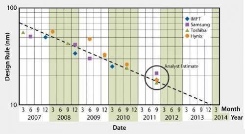
Figure 1: Trends in the manufacturing process geometry of NAND flash
For consumer storage applications, the most common solid-state memory format is SD flash memory. The current SD flash is based on NAND technology and has three dimensions, as shown in Figure 2, namely SD card, mini SD card and micro SD card. Although these three dimensions are of different sizes, their interfaces are the same.
In addition to the dimensions, SD memory can also be classified by capacity. Standard SD card can provide up to 2GB of capacity, large capacity (SDHC) card capacity of 2 to 32gb,extended capacity (SDXC) cards as high as 32GB to 2TB.
Besides, SD memory has two types of clock frequency. In the default mode, the memory can work at a clock frequency of 0 to 25MHz, with an interface speed of up to 12.5MB/s (using 4 parallel data lines). In high-speed mode, the memory can operate at a clock frequency of 0 to 50MHz, with an interface speed of up to 25MB/s (using 4 parallel data lines). System designers can optimize this parameter based on the desired read and write speed, which becomes important when discussing power considerations.
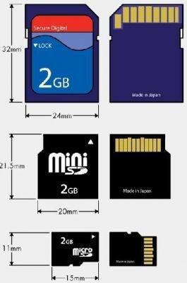
Figure 2: Dimensions of SD card, mini SD card, and micro SD card
SD specification version 2.0 requires operating voltage range from 2.7 to 3.6V. 2.7V is the minimum voltage required to ensure performance, while operating voltage from 2.7V to 3.6V is acceptable, but if more than 3.6V, the performance is not guaranteed, and the memory may be compromised.
Another consideration in power supply design is the consumption of memory. Memory has four main working modes: interrupt, standby, read and write, and power consumption is also different in different states. For a given memory card, the power consumption of the read/write state is also related to the speed. Common card can support clock frequency of up to 25MHz clock frequencies, while high-speed card supports up to 50MHz. As storage capacity grows, faster clock frequencies are required to ensure proper consumer usage patterns.
For low-speed and small-capacity SD cards, power consumption is often less than 100mA. Assuming that the rated working voltage of a lithium-ion battery is 3.7V and the power rail of memory is quite high, the linear regulator becomes the power choice for SD memory. However, the selected linear regulator must be able to work in a low voltage drop (LDO) mode, as the effective voltage of lithium-ion battery ranges from 3.2 to 4.2V.
With the advent of 8, 16, and 32GB high-speed SD cards, 300 to 400mA of power consumption has been common, significantly larger than the 100mA of small capacity cards. As a result of larger current requirements, the power consumption of LDO power solutions began to increase significantly. Figure 3 shows an LDO regulator that provides a typical 2.9V to an SD card. 2.9V is selected here because it is assumed that LDO ensures that the output is no less than 2.7V at any lines, loads, or temperature conditions.
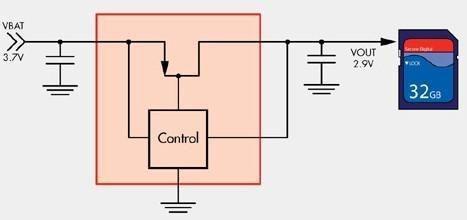
Figure 3: An LDO regulator that provides a typical 2.9V to an SD card
Table 1 lists the conversion efficiency of LDO in the case of 300mA and 400mA output currents shown in Figure 3. The calculated LDO conversion efficiency is 78%, so the power consumption is 240mW and 320mW, respectively.
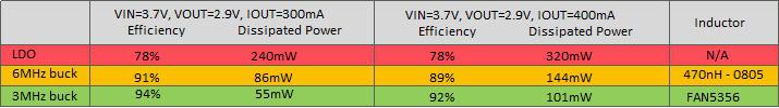
Table 1: Comparison of power efficiency and power consumption among LDO, 6MHz buck converters, 3MHz buck converters
However, many system designers believe that 320mW or even 240mW of power consumption is unacceptable. Fortunately, the switch converter shown in Figure 4 can now be used to achieve higher power conversion efficiency.
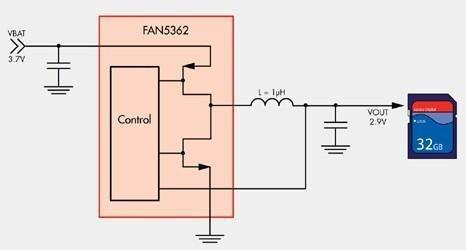
Fig 4: FAN5362 buck converter realizes 2.9V of power supply circuit in SD card.
As calculated in table 1, for 300mA systems, FAN5362 can reduce power consumption to 55mW, and for 400mA systems, FAN5362 can reduce power consumption to 101mW. These efficiency values are obtained according to the measured FAN5362 efficiency curve. Figure 5 shows the efficiency curves of AutoOPFM (solid lines) and ForcePWM (dotted line). While optimizing FAN5362 efficiency, 3MHz is selected as the rated switching frequency because it can provide the best trade-off between size and efficiency. As can be seen from table 1, for this power-sensitive application, the power consumption of the 6MHz switching frequency is much greater than that of 3MHz.
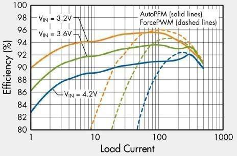
Fig 5: The relationship between FAN5362 efficiency and load current. AutoPFM is solid line and ForcePWM is dotted line.
Although it does not seem significant to choose a buck converter to replace LDO, it becomes important to consider that the buck converter must be able to work at a very high duty cycle. If the output of the buck converter is set to 2.9V and the battery voltage is as low as 3.3V, the buck converter works at 88% duty cycle. Under certain load and input voltage conditions, the buck converter will even be forced to stop the switch and work at 100% duty cycle. If mobile phone starts emitting GSM pulses, this situation will become more severe in the case of low battery voltages (VVBAT). GSM pulse may be as high as 2 A, and during these pulses, the output impedance of lithium-ion battery will drop the battery voltage by 400mV. For LDO, a sudden drop in VVBAT is beneficial because LDO always work in linear areas. But for buck converters, the situation is different, because they have to gradually change from switching state to 100% conduction. Once the battery voltage returns to 3.3V, it will return to switching state. During this period, the high-side device is fully conductive, and the output voltage of buck converter is only VVBAT– RDS(ON) *I – DCR*I, where RDS (ON) is the conduction impedance of the high side FET, DCR is the serial impedance of the inductor, and I is load current of the memory.
FAN5362 is specially designed to handle the minimum overshoot/undershoot described above. In addition, control mechanisms of FET and RDS (ON) are carefully designed to ensure that the output voltage is never less than 2.7V, even including transient responses of line and load. This is critical for memory, as the SD Specification version 2.0 requires operating voltage ranges between 2.7 and 3.6V.
Although advances in process geometry have met the need for ultra-compact and low-cost SD memory, this large-capacity device also brings power problems. This challenge can be addressed by replacing the current LDO with products such as buck converter FAN5362, which is designed specifically for such applications. Figure 6 is a typical schematic diagram and PCB layout of the complete FAN5362 power solution.
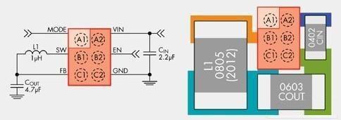
Figure 6: Typical schematic diagram and PCB layout of FAN5362.