
Explain the principle and use of NAND Flash with examples (1)
Guide: This article takes Micron MT29F2G08 as an example to introduce principle and use of NAND Flash. NAND's internal storage array is accessed on the basis of pages.
This article takes Micron MT29F2G08 as an example to introduce principle and use of NAND Flash.
1. Overview
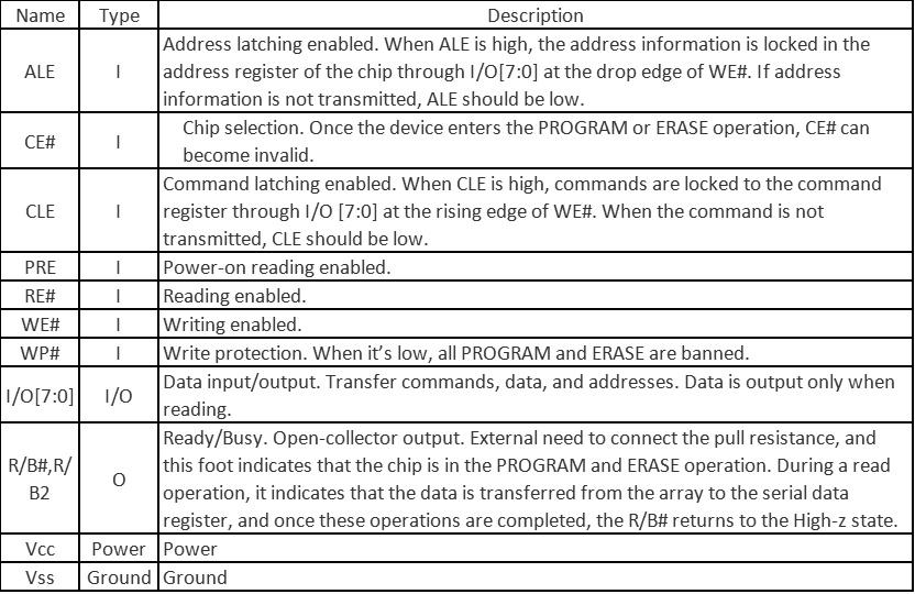
MT29F2G08 uses a highly multiplexed 8-bit bus (I/O[7:0]) to transfer data, addresses, and instructions. Five command feet (CLE, ALE, CE#, WE#) implement NAND command bus interface protocol. Three additional feet are used to control hardware write protection (WP#), monitor chip status (R/B#), and initiate power-on auto-read features (PRE-only 3V chip support). Note that the PRE function is not supported on extended-temperature chips.
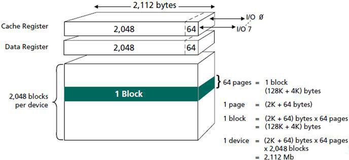
There are 2048 erasable blocks inside MT29F2G08, each of which is divided into 64 programmable pages. Each page contains 2112 bytes (2048 bytes as data storage area, and 64 alternate bytes generally as error management).
Each 2,112-byte page can be programmed within 300us, and each block (64x2112=132K) can be erased within 2ms. On-chip control logic automatically carries out PROGRAM and ERASE operations.
NAND's internal storage array is accessed as a basic unit of page. When reading, a page of data is copied from the internal storage array to the data register, and then output in bytes from the data register. When writing (programming), it is also based on the page: after the starting address is loaded into the internal address register, the data is written sequentially to the internal data register, and after the page data is written, the array programming process starts.
To increase the speed of programming, the chip has a cache register. In cache programming mode, data is first written to the cache register, then to the data register. Once the data is copied into the data register, programming begins. After the data register is loaded and programmed begins, the cache register becomes empty and can continue to load the next data. Therefore, the internal programming and data loading are carried out in parallel, improving programming speed.
Internal data move commands also use internal cache registers, which typically takes a long time to move. By using internal cache registers and data registers, the data is moved much faster and does not require using external memory.
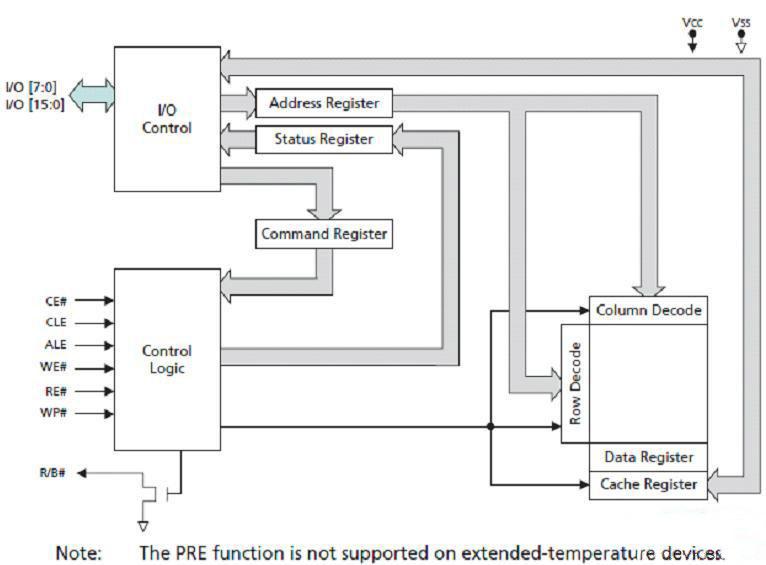
2. Functional block diagram
3. Pins
4. Addressing
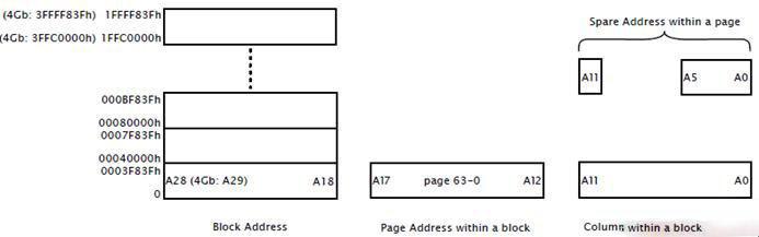
Block address and page address is equal to actual page address. Hopefully, through this diagram, we can understand block, page, block address, page address, column address, backup space, backup address.
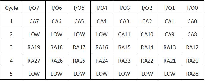
CAX: Column Address; RAx= Row Address