
How many process will be from sand to Wafer ?
Why can the sand be used as raw material to make wafers?
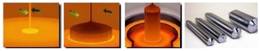
The main reason for choosing the sand is that the main component of the sand is SiO2 and the raw material of semiconductor is silicon (Si), so it is directly extracted from the sand. First, the sand (SiO2) is displaced with carbon at a high temperature (2000C) to form silicon and CO2. At this time the silicon is metallurgical grade (MGS: Metallic Grade Silicon), namely coarse polycrystalline silicon. After further purification of polycrystalline silicon, the purified TCS is reacted with H2 at 1100 C to form electronic grade (EGS: electric grade silicon) polysilicon and HCl, and then the monocrystalline silicon is made.
How do you go from a silicon ingot to every silicon chip?
1. Trimming/cutting: All wafers have a Notch (the flat is 6-inch), which is cut when the ingot is done. It must be cut along <110>, so the Notch orientation is specified as 110+/-1deg in the Wafer specification. The depth of the notch and the size of the flat are all specified by SEMI M1. There are two kinds of flat for 6 inches, generally 47.5mm and 57.5mm, depending on your machine. The 8-inch wafer notch is uniform with a depth of about 1 to 1.25 mm, an angle of ~90 deg, and a radius of 0.9 mm.
2. Cutting the silicon ingot into a wafer: linear cutting (many pieces can be cut at one time) is adopted. The knife rotates, while the silicon ingot only translates without rotation because of the large contact area of the concave blade. The reason why the ingot doesn’t move is that the notch is afraid of being hit by the knife edge. The thickness of each wafer is determined by the distance between two blades, generally 4 inches for 525mm, 5 inches for 625mm, 6 inches for 675mm, 8 inches for 725mm, and 12 inches for 775mm.
3. Edge rounding: The edges of the freshly cut wafer must be sharp cylinders that need to be rounded to reduce stress. Rotate the wafer in a fixed slot and grind it like a knife.
4. Lapping: Because wafers that have just been cut must have a lot of damage and a rough surface, this step is similar to CMP, grinding with slurry. Thus, the wafer is sometimes called the polish wafer.
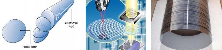
5. Wet etching: The polishing is still mechanical and the damage cannot be completely removed, so that a further chemical reaction is required to remove the surface defects. The adopted dosage ratios of HNO3/HF/CH3COOH(acetic acid) is mainly 4:1:3. The SiO2 can be oxidized by nitric acid and corroded by HF.
6. Annealing: Annealing can remove the lattice damage. The gas Ar is usually used, so we sometimes see our flow using Ar to anneal wafers. The reason for using Ar instead of H2 is because Ar is an inert gas without reaction and H2 was previously said to cause a change in its surface concentration.
What is a wafer?
The wafer is made of pure silicon (Si), generally divided into 6 inches, 8 inches and 12 inches in size. Samsung, Toshiba, Western Digital, Micron and other purchase silicon wafers made into NAND Flash and DRAM wafers. Due to the different nanotechnology used by each manufacturer, the NAND Flash chips differ in performance and cost.
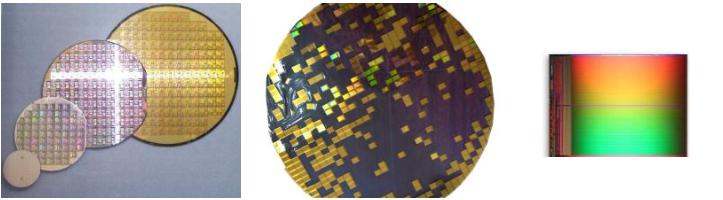
Once made into a NAND Flash wafer, the wafer is cut into one chip after another, called Dies in professional term. The capacity unit of a single Die is Gbit, different from the chip unit of Gbyte because 1Byte=8 bit.
Once made into a NAND Flash wafer, the wafer is cut into one chip after another, called Dies in professional term. The capacity unit of a single Die is Gbit, different from the chip unit of Gbyte because 1Byte=8 bit.
After cutting and testing, Samsung, Toshiba, Western Digital, Micron, etc. will divide the Flash Die into qualified and unqualified. The qualified Flash Die will be packaged and the unqualified Downgrade Wafers, some residual leftover material, will be done scrapping by the original factory. Many of the unqualified Downgrade Wafers, known as the black piece of Ink Die, will be processed in the form of blue film Wafers to downstream packaging plants for processing and recycling, and finally used by some small manufacturers for cheap bundles of SD cards and U-disk, etc..
The original factory stacks and encapsulates Good Die into different NAND Flash chips, and then packages them with the control chips to produce eMMC products. The eMCP is made by packaging eMMC and LPDDR into multiple chips, and then used in terminal products such as mobile phones, tablets and smart boxes. The SSD, made up of one or several NAND Flash chips on the PCBA board and control chips or DRAM chips, is mainly used in computers and servers.