
Learn about every aspect of photoresist (3)
3. Evolution of photoresist
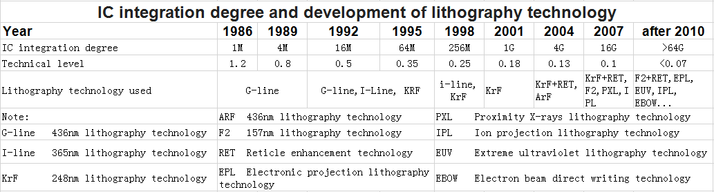
With the requirement of miniaturization and functional diversification of semiconductor products in the market, semiconductor photoresist continuously improves the limit resolution by shortening the exposure wavelength, so as to achieve higher density of integrated circuits. As IC integration improves, its process level in the world has changed from micron, submicron and deep submicron to nanometer.
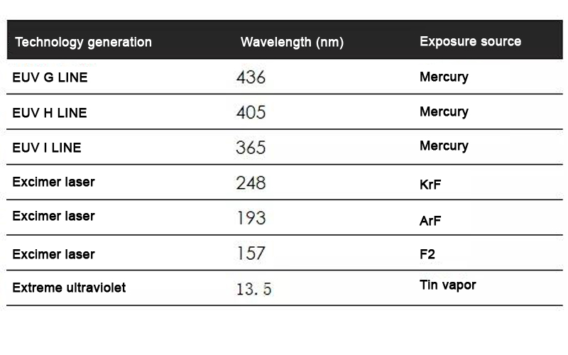
In order to meet the requirement of shrinking the line width of integrated circuits, the wavelength of photoresist is shifted from ultraviolet spectrum, G-line (436 nm), I-line (365 nm), KrF (248 nm), ArF (193 nm), F2 (157 nm) to EUV. Besides, the resolution of photoresist is continuously improved by resolution enhancement technology.
At present, the main photoresist used in semiconductor market includes G-line, I-line, KrF and ArF photoresist, of which G-line and I-line photoresist are the most widely used in the market.

R is the minimum feature size, that is, the minimum distance that can be distinguished. K1 is a constant, also known as Rayleigh constant. λ is the wavelength of the exposure source and NA is the numerical aperture of the lens. Therefore, we can see that the way to further reduce the minimum feature size is to reduce the wavelength of the exposure source and increase the value of NA.
The method of reducing exposure wavelength is multiplied by the development history of lithography. The wavelength is from UV to DUV, and the light source is from high pressure mercury lamp to stimulated excimer laser. The most attractive EUV photoresist launched by ASML uses plasma tin vapor as light source, whose wavelength is reduced to 13.5 nm. However, the whole lithography needs to occur in vacuum environment, so that the production speed is low.
The pursuit of higher resolution exposure sources has also led people to think of two kinds of non-optical sources: X-ray and electron beams. At present, electron beam lithography is a mature technology, which is used to produce high-quality mask and amplified mask.
Different from the traditional mask lithography, this method uses electron beam and computer to control directly "writing", and can achieve a resolution of 0.25 micron at present. Similarly, this method is slow to produce and needs to be realized in vacuum environment.
X-ray with a wavelength of only 4-50 Å is an ideal light source, but X-ray can penetrate most of the masks and the development of X-ray photoresist is so difficult that it has not been used.
In addition to improving NA, people have also come up with a method. Immersion lithography greatly increases the numerical aperture NA by replacing the medium between lens and photoresist with other substances expect air, further greatly improving the resolution of lithography without changing the exposure source. 193 nm technology can meet the requirement of 45 nm process nodes, but can achieve 28 nm process nodes through immersion technology.
The combination of immersion and dual exposure reduces the process nodes of 193nm lithography to 22nm, and reaches 10nm process node limit, which makes 193nm lithography continue to be widely used in the market.

The application of photoresist must keep pace with the development of lithography. With the continuous upgrading of exposure light source of lithography, photoresist has also changed from ultraviolet negative photoresist (cyclized rubber negative photoresist) to ultraviolet positive photoresist (DNQ - Novolac positive photoresist), and then to deep ultraviolet photoresist (chemical amplified photoresist (CAR)).
(1) Ultraviolet negative photoresist
In 1954, EastMan-Kodak synthesized first photosensitive polymer, namely polyvinyl alcohol cinnamate (PVA-cinnamate), and created the photoresist system of PVA-cinnamate and its derivatives. This is the earliest photoresist used in the electronic industry. In 1958, Kodak developed the cyclized rubber- bihydrazoates photoresist.
Because of its good adhesion to silicon wafers, fast photosensitivity and strong resistance to wet etching, it became the main photoresist in the electronic industry in the early 1980s, accounting for 90% of the total consumption at that time.
However, developing with organic solvents can cause the swelling of the film, further limiting the resolution of the negative photoresist. Therefore, negative photoresist is mainly used in the fabrication of discrete devices and 5um or 2~3um integrated circuits. With the continuous improvement of integrated circuit integration, although the application of negative photoresist is gradually replaced by positive photoresist, there are still many applications in the field of discrete devices.
(2) Ultraviolet positive photoresist
The phenolic resin-diazonaphthoquinone positive photoresist developed around 1950 is developed with dilute alkali water. Due to no film swelling problem during the development, it has high resolution and strong resistance to dry etching, meeting the requirements of large-scale integrated circuits and ultra-large-scale integrated circuits. According to using different exposure machine, ultraviolet positive photoresist mainly used in integrated circuit manufacturing and LCD manufacturing can be divided into broad-spectrum ultraviolet positive photoresist (2-3um,0.8-1.2um), G-line positive photoresist (0.5-0.6um), and I-line positive photoresist (0.35-0.5um).
Beyond G-line photoresist in the mid-1990s, I-line photoresist is the most widely used photoresist at present. With the improvement of I-line lithography, I-line positive photoresist can be made up of integrated circuits with a line width of 0.25um, which prolongs the service life of I-line technology. In a typical device, one third of the layers are the real key layer, one third of the layers are the sub-key layer, and the other is the non-key layer. There is a hybrid matching lithography method that matches photoresist and equipment technology with the critical state of the silicon wafer layer. For example, for 0.22um DRAM devices, I-line stepping lithography can form a total of 20 layers on the device, 13 layers among which are key layers and the remaining 7 layers imaged by front-end deep ultraviolet stepping scanner. In addition, the use of I-line can reduce production costs, so I-line lithography will continue to occupy a certain market share for a long time.
(3) Deep ultraviolet photoresist
Unlike ultraviolet photoresist, deep ultraviolet photoresist is chemical amplified photoresist (CAR). The characteristics of CAR are as follows. First, add photoacid-producing agent in photoresist. Then, acid-producing agent decomposes into acid under light irradiation. During banking, acid acts as catalyst to remove protective group (positive photoresist) from film-forming resin or to catalyze cross-linking reaction (negative photoresist) between cross-linking agent and film-forming resin.
After the removal of protective group or cross-linking reaction, acid can be re-released without being consumed, and can continue to play a catalytic role, greatly reducing the energy required for exposure and improving the photosensitivity of photoresist.
The research of 248nm photoresist with KrF excimer laser as exposure source originated around 1990 and entered a mature stage in the middle and late 1990s. At present, the most widely used photoacid-producing agents in CAR are non-ionic photoacid-producing agents or onium salts that can produce sulfonic acid. The main functional polymer is esterified polyhydroxystyrene.
248nm photoresist is developed with KrF excimer laser for line width of 0.25 um, 256M DRAM and related logic circuits. By increasing the NA value of exposure machine and improving the matching lithography technology, it has been successfully used in the fabrication of line width of 0.18-0.15 um, 1G DRAM and related devices. Besides, after using resolution enhancement techniques such as phase-shifting mask, off-axis illumination, proximity correction and others, 248nm photoresist can make images less than 0.1 um, resulting in entering 90nm nodes era.
These results indicate that 248 nm photoresist technology has entered a mature stage.
The photoacid-producing agent used in ArF 193nm far-ultraviolet chemical amplified corrosion inhibitor is roughly the same as 248nm far-ultraviolet photoresist. In functional polymers, the film-forming resin used in 248nm far- ultraviolet photoresist has strong absorption at 193nm because of the benzene ring, however, this type of film-forming resin can not be used in 193nm far-ultraviolet photoresist.
The main resin of 193nm photoresist is required to be transparent at 193nm wavelength, with good adhesion to the substrate and high vitrification temperature (generally 130-170 ℃). Chemical amplified imaging photoresist must also have acid-sensitive side-hanging groups to improve its imaging ability. The commonly used 193nm photoresist materials can be divided into acrylates, polycyclic olefin adducts, cyclic olefin-maleic anhydride copolymers, silicon-containing copolymers, multicomponent copolymers and small molecular materials.
At present, 193nm photoresist is the mainstream solution in the market, and it is also the most advanced solution before the commercialization of EUV.
(4) Next generation of EUV photoresist
When EUV lithography in progress needs to be equipped with special photoresist, the technology of EUV lithography also puts forward quite stringent requirements for EUV photoresist. EUV photoresist should be characteristic by low absorbance, high transparency, high etching resistance, high resolution (less than 22 nm), high sensitivity, low exposure dose (less than 10 mJ/cm 2), high environmental stability, low gas production and low line edge roughness (less than 1.5 nm).
Since this technology uses a light source with a wavelength of only 13.4 nm, it requires that the high absorption elements (such as F) should be minimized in the main materials, and that increasing C/H ratio will also help to reduce the absorption of materials at 13.5 nm. According to the review of the research progress of photoresist mentioned by Beijing Molecular Science Laboratory and Chinese Academy of Sciences Chemistry, it is pointed out that there are three main types of photoresist systems in EUV lithography.
Non-chemical amplified polymer system, molecular glass system and polymer (or small molecule) - PAG system, etc.