
Practical guide for flash memory
Asynchronous timing
The flash interface is divided into synchronous and asynchronous. Generally speaking, the asynchronous transmission rate is slow and the synchronous is fast. Since the asynchronous interface has no clock, each data read is triggered by a RE_n signal, and each data write is triggered by a WE_n signal. The difference is that the synchronous interface has a clock signal, data read-write synchronizing with the clock.
Let's first take a look at a typical flash chip pin diagram specified by the ONFI2.3 protocol, where the external data output of this chip is 8-bit width. Ssync is synchronous, and Async is asynchronous.
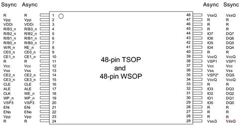
Figure 1-1 The flash chip pin diagram
Compare the pin definitions of the two interfaces. Most of them are the same, the difference being the four types of signals in Table 3-3. We can see why these signals are different later by looking at the timing of synchronization and asynchrony.
Table 1-1 Comparison of pin definitions between synchronous and asynchronous
Synchronous | asynchronous |
W/R_n | RE_n |
CLK | WE_n |
IO7-0 | DQ7-0 |
VSP2 | DQS |
Let's take a look at the timing diagram for asynchronous data write.
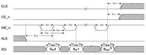
Figure 1-2 Asynchronous data write timing diagram
There are 5 signals in this picture:
CLE: Command Latch Enable. When CLE is valid , IOx sends commands
CE_n:Chip Enable. The signal selects a logical chip - Target. Why is it a logical chip? The physical chip encapsulates many Targets, each of which is completely independent, but it is possible to share the data signals. Therefore, CE_n is used to select which Target is currently transmitted by the data. The industry generally refers to Target as CE.
WE_n:Write Enable. The signal is sent to the flash memory by the user. When it is valid, it means that the data write sent by the user can be sampled.
ALE:Address Latch Enable. IOx sends address when ALE is valid
IOx: Data Bus
There are a lot of time parameters at the same time. Here are only a few key parameters:
tWP is the width of the WE_n low-level pulse, while tWH is the high-level holding time of WE_n. The time of one cycle is tWC;
tDS is the data establishment time, which means that the 8-bit data should reach a steady state at most such a long time.
tDH is the data stability time, during which the data signal is stable and can be sampled.
So we look at the timing diagram above. When data is written, the data bus can’t transfer addresses and commands, so ALE and CLE are invalid. While the Target transfers the data, CE_n is valid. Each WE_n cycle corresponds to a valid data transmission.
Let's take a look at the asynchronous data read timing diagram. There are two more signals:
RE_n:Read enable. This signal is sent by the user to the flash memory. Each time a read is enabled, the flash memory prepares data on the data bus for the user to sample.
R/B_n: Ready/Busy. When the flash is being read internally, Busy_n is valid. When the data is available, Ready is valid and the user can read it.
Thus, the graph is that after the user sends a read command to the flash memory, the Ready signal goes up, meaning the data is ready and then, the user sends a RE_n signal to read the data. For each RE_n cycle, the flash sends a valid data to the data bus for the user to sample.
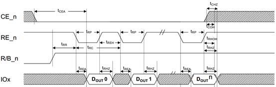
Figure 1-3 Asynchronous data read timing diagram
Synchronous timing
The two most important signals in synchronous timing are the clock CLK and DQS. Current flash memory basically uses DDR (Double Data Rate) technology, which means that two dials of data are transmitted every clock cycle. Figure 3-35, a data write timing diagram in synchronous mode, introduces several signals.
CLK: Clock. The clock signal is generated by the user. Data is triggered on both the rising and falling edges of the clock signal to implement DDR, which means that the data transmission rate of 100MHz clock frequency is 200MT/s.
W/R_n: Write/Read_n. The electrical level is high when writing, and the level is low when reading.
DQS: Data Strobe. DQS is used to distinguish each data transmission period, so that the receiver can receive data accurately. When reading data, DQS is generated by flash memory and the upper and lower edges of DQS are aligned with the data. When writing data, DQS is generated by the user and the middle of the DQS corresponds to the intermediate stable area of the data. Therefore, DQS can be regarded as a synchronization signal of data.
DQ[7:0]: Data Bus
Let's take a look at a few key time parameters.
tCALS: The establishment time of CLE, W/R_n and ALE.
tDQSS: The time of data input to the first DQS hopping edge.
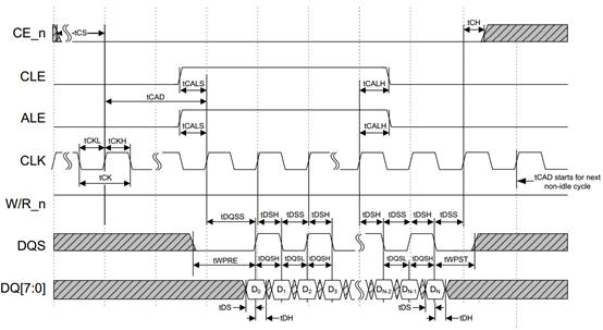
Figure 1-4 Synchronous data write timing diagram
After knowing the various signals and time parameters, we can understand the above data write timing diagram. After CLE and ALE are valid, the data is ready and output at the first CLK rising edge. After the tDQSS, the DQS begins to hop and the edge of the hopping is at a stable position of the DQ data signal. A set of data is output every half of the clock cycle later.
Let's take a look at the following data read timing diagram (Figure 3-36), which is similar to the data write timing diagram except that the W/R_n signal is low and the DQS hopping edge is synchronized with the rising edge of the data.
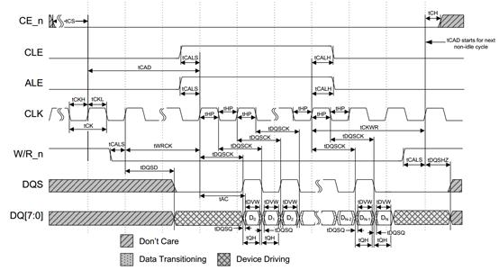
Figure 1-5 Synchronous data read timing diagram
Flash command set
The main control of SSD communicates with the flash through a series of flash commands. Each flash chip defines the commands it supports. The commands defined are shown in Table 3-4 in the case of the ONFI 2.3 protocol. When the users want to use these functions, they can just send commands, for instance, reading data only requires sending 00h-30h. However, the specific command timing and usage depend on the specific definitions.