
The development of Moore's Law from the perspective of 8-year evolution of Core
01 From "Tick-Tock" model to "PAO" model
Starting with Broadwell in 2014, the Intel Core processor has officially entered the era of 14nm process. There has been little substantial progress in the manufacturing of the Core processor over the next four years, for instance, Skylake in 2015, Kaby Lake in 2016, and Core 8 with multiple micro-architectures in 2017 are all based on the 14nm process. Although 14nm process is divided into 14nm, 14nm+, and 14nm++ based on energy consumption, they are never separated from the 14nm node, and even the upcoming 9000 series processors are likely to be 14nm process.
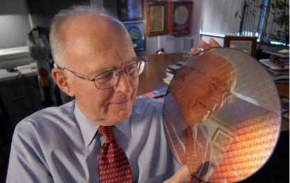
Gordon Moore, one of Intel’s founders, put forward Moore's Law.
Moore's Law, which has been adopted by the semiconductor industry for half a century, has been guiding the growth rate of silicon transistor density from “doubling every year” to “doubling every 18 months”. Gordon Moore, the proponent of Moore's Law, wrote the myth of the semiconductor industry with his unique forward-looking perspective. However, when the time is approaching the second decade of the 21st century, the pace of the CPU process slowed down – 14nm has already been used in the four generations of Core processor. Does that mean Moore's Law is no longer working?
To answer the question of whether Moore's Law is invalid, let's review the processes used by Intel’s Core processors. (This article only discusses the Core i processor released in 2010)
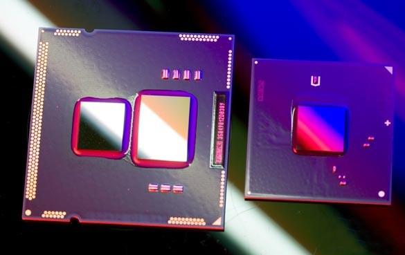
The left is a Clarkdale micro-architecture processor that encapsulates CPU and GPU independently.
Intel introduced the Core i series processor based on Westmere micro-architecture in 2010. Clarkdale, the mainstream desktop platform, was claimed by Intel as the first-generation Core processor, mainly because it first encapsulated the GPU graphics core in the processor. When the CPU and GPU were still two independent Die at the time, it is undeniable that Clarkdale pioneered the integration of CPU and GPU. Besides, it is also the first time to apply the 32nm process in the CPU.
The “Tick-Tock” model
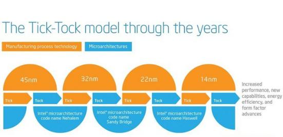
According to the iterative strategy of the Intel’s "Tick-Tock" model, the Westmere micro-architecture is part of the "Tick" process to update the process technology of the processor, while Sandy Bridge emerged one year later belongs to the "Tock" process to update the micro-architecture of the processor based on the upgrade process technology. The "Tick-Tock" model, officially introduced in 2007, is steadily moving forward at the pace of the biennial update of process technology.
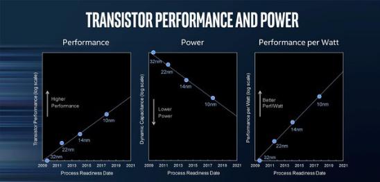
More advanced processes technology leads to higher energy consumption.
In the following four years, Core processors have ushered in the 22nm process of Ivy Bridge, Haswell and 14nm process Broadwell, Skylake. Although the processor continues to improve performance with the help of more advanced process technology and micro-architecture, the power consumption is gradually decreasing, that is, the performance per watt of the CPU is gradually increasing.
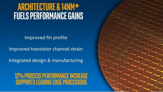
14nm+ process improves fin height and gate spacing
However, Intel's "Tick-Tock" model seemed to be in trouble in 2006. Kaby Lake, which was supposed to use 10nm process at the time, was still hovering at the 14nm. Although Intel added a "+" suffix after 14nm and advertised that it achieved less driving current and better heat control by improving the fin height and gate spacing, this still does not dispel concerns about the outlook of Moore's Law.
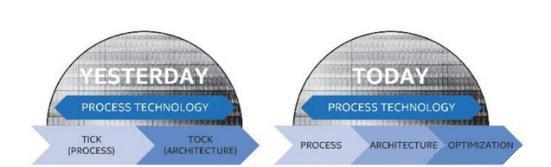
"Tick-Tock" model is transformed into "PAO" model
More seriously, the launch of Kaby Lake directly declared the death of the "Tick-Tock" model, and the pace of the biennial update of process technology is no longer applicable to the iteration frequency of the processor. In order to find a more reasonable explanation, Intel has come up with three-step process development strategy of "Process, Architecture, Optimization". In this way, Kaby Lake has a seemingly perfect foothold - optimization.
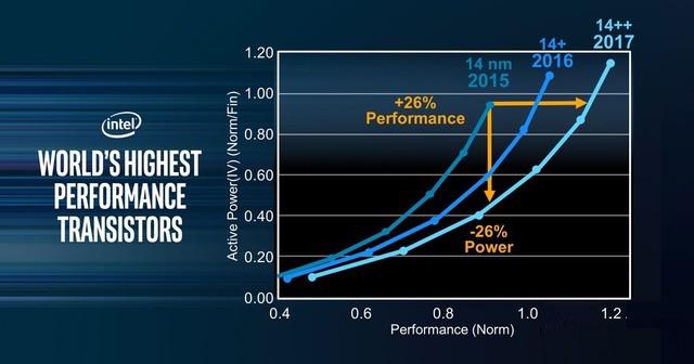
Energy consumption relationship between three generations of 14nm
If Kaby Lake is the optimization part of the “PAO” model, then according to this idea, the next Coffee Lake should move into a new round of upgrades. But contrary to expectations, Coffee Lake was still 14nm, and added a "+" to Kaby Lake 14nm+ to turn into 14nm++, which makes the "PAO" model a little embarrassing.
02 Is Moore's Law really a law?
From the "Tick-Tock" model proposed in 2007 to the "PAO" model in 2016, the Core processor did not strictly follow the established route to upgrade the process technology, and even gradually deviated from the periodic exponential growth of the number of silicon transistors defined by Moore's Law. It’s necessary for us to understand what Moore's Law is before discussing what blocks the progress of processor.
Gordon Moore predicted that the chip will contain 65,000 transistors by 1975.
To be exact, Moore's Law is not a strictly physical law, but a prediction of future trends based on observations of existing technologies. Gordon Moore, an engineer at Fairchild Semiconductor, wrote in the journal of Electronics in April 1965, "As the number of components in each circuit increased, the unit cost dropped. As many as 65,000 transistors could be packed onto a single silicon chip by 1975. More commonly, the number of transistors in a chip doubles every year.”
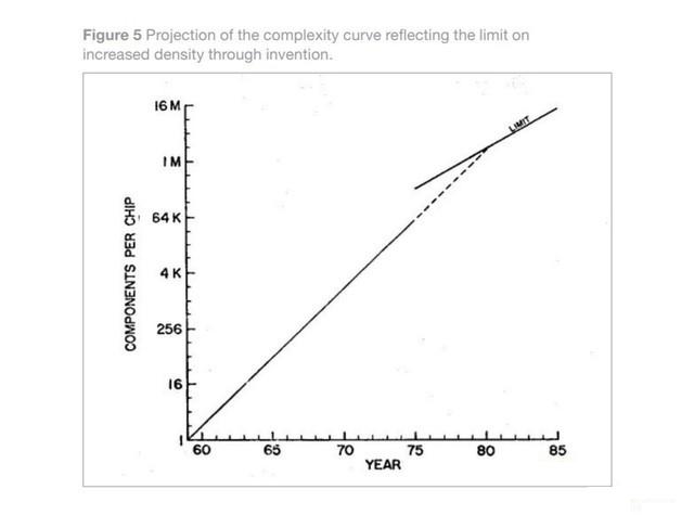
Moore corrected the growth slope of the number of transistors per chip in 1975.
Importantly, Moore's Law is not changeless, but is adjusted according to the different circumstances of the times. Moore has revised the previous idea in a paper submitted at the IEEE International Electron Devices Meeting in 1975: “In the next decade, as the machinery used to develop technology becomes more expensive, the “doubling every year” will slow down to “doubling every 18 months”, and there will be 16 million transistors on a chip by 1985.”
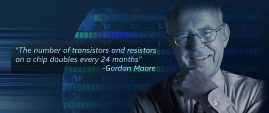
Another way of saying Moore's Law: the number of transistors on a chip doubles every 24 months.
From Moore's two rhythmic growth predictions about the complexity of silicon transistors, we can generally conclude that Moore's Law is a constantly evolving and gradually improving prediction about the growth rate of the number of transistors per chip. This prediction is not indefinite, but a tentative vision for the next 10 years. From this perspective, it seems inappropriate to use Moore's Law 40 years ago to measure the frequency of upgrading the current processor process.
03 The limits of transistors are insurmountable.
However, it is an indisputable fact that the CPU process has slowed down according to the Core processor process technology in the last four years, especially in 2016. The 14nm process that has been extended to the four generations of Core processor has already shown the weakness of the advancement. Moreover, the "+" suffix has been used twice. We can't help but ask, what is the obstacle to the advancement of the processor process?
“All excellent exponential growth will come to an end.” As a pioneer in the digital revolution in Silicon Valley, Gordon Moore not only predicted the growth trend of silicon transistors, but also foresaw that silicon transistors would not grow endlessly but encounter a fundamental obstacle.

Atomic schematic
As we all know, atoms are the smallest particles in chemical changes. Thus, a transistor printed chemically can not go beyond the atomic limits. That is to say, it is impossible to chemically print a function smaller than an atom, which is the most fundamental reason for the growth of silicon transistors.
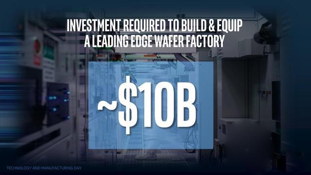
The investment required to build and equip a leading-edge wafer factory will exceed $10 billion.
In addition, increasingly stringent manufacturing processes have led to increasing research and development costs, which are enormous for each generation with more advanced processes. According to data previously released by Intel, the investment required to build and equip a leading-edge wafer factory will exceed $10 billion. What is $10 billion? It is about one third of AMD’s total market value.
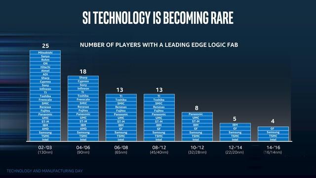
Silicon semiconductor technology is becoming rare.
As the threshold for semiconductor manufacturing technology and R&D capital becomes higher and higher, the number of enterprises with wafer production capacity is gradually decreasing. 21 wafer manufacturers have been eliminated in the past 15 years, from 25 in 2002-2003 to 4 in 2014-2016. By the end of last month, GlobalFoundries (GF) announced that it would put aside the research and development of 7nm and below processes, and integrate resources into the more mature 12nm/14nm process, due to the huge R&D capital required for the new process.