
The new type of DRAM breaks the refresh limitation with VLT technology
Vertical Layered Thyristor called VLT, a new memory unit developed by Kilopass, is able to significantly reduce the cost and complexity of DRAM. This is a static memory unit that does not require refresh operation; it is compatible with existing manufacturing equipment of fabrication plants, and does not need any new materials or technologies.
Compared to DRAM, VLT memory arrays can save 45% of the cost. This is because it has a smaller VLT memory unit and the ability to drive longer rows and columns, allowing it to greatly improve the efficiency of memory arrays. However, to take advantage of VLT, manufacturer must design and produce in a mature DRAM market developed by professional industry standard, which is necessary for maintaining compatibility with memory products from different suppliers.
Currently, memory based on VLT technology is fully compatible with existing " fourth generation double data rate of low power" (LPDDR4) specifications. VLT bank can simulate the bank of traditional DRAM and be compatible with its frequency. When designing the VLT circuit, the designer can choose to connect the standard DDR controller, or a simplified controller at a lower cost. If you use a standard controller, the VLT memory will ignore the refresh sequence because there is no need to refresh. Other parts of the system will treat VLT DRAM as generic DRAM, so no changes will be needed.
The traditional storage unit of DRAM
To show how to use VLT memory units to construct LPDDR4 memory, first let's review how traditional DRAM and LPDDR4 work. Those who are familiar with DRAM may have some knowledge of it, but there are some slight differences in actual application. Therefore, some standards and terms are defined in advance for understanding.
Many aspects of DRAM operation depend on its capacitance storage unit. Firstly, the characteristics of leaking electricity of capacitance makes it necessary to refresh. Secondly, the basic working way of storage unit is reading, which would affect how to organize memory in other aspects.
Figure 1 shows the schematic diagram of the capacitance storage unit, and the left and right diagrams respectively represent the situation when reading 1 and reading 0. The circuit detects the place value of memory through charge sharing. Bitline is firstly precharged to a voltage value between 0 and 1, and then selects a memory unit by turning on the reading transistor, so that the charge can flow between the bitline and the memory unit. If the voltage of bitline is higher than the memory unit, the negative charge will flow out of the memory unit to the bitline. If the voltage of the bit line is lower than the memory, the negative charge will flow from the bitline into the memory unit.
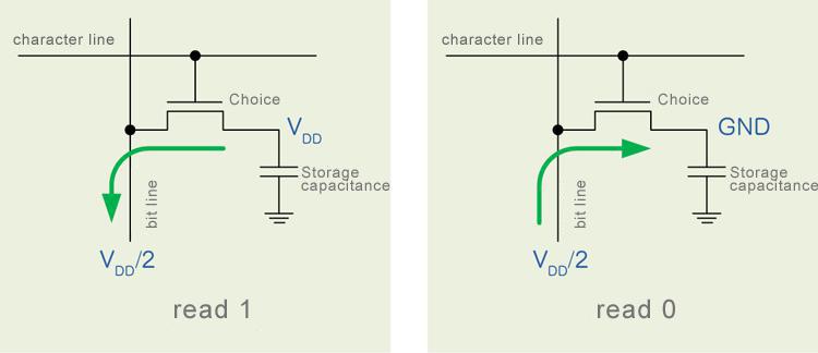
Picture 1:The charge distribution principle of conventional capacitive DRAM memory units (the green arrow in the figure shows the direction of electric current, which is opposite to the direction of the negative charge flow)
This transfer of charge changes the voltage on the bitline, and the final value is obtained through sensing and latching. However, the loss or gain of the charge in the storage capacitance changes the original charge on the node, which means the reading process is destructive. Therefore, after each reading, the charge in the memory unit must be regained through the write back operation.
LPDDR4
The LPDDR4 standard is a low power version of the fourth generation double data rate (DDR) DRAM, which defines the high-level structure of individual memory chips through the overall architecture and how to arrange the dual in-line memory modules (DIMM).
There are two ways to analyze DRAM: theoretically, analyze its physical details; practically, look at its array characteristics. This article firstly explores the first logical view, since all entity arrangements must be decomposed into the same logical structure, from which you can learn how traditional DRAM and LVT approaches achieve logical functions.
The LPDDR4 memory chip has a storage capacity of 8Gb and usually consists of two separate 4Gb channels. Each channel has 8 memory groups, each of which includes 32K storage pages (page) and 16K bits per page, so that the total capacity of memory group up to 512Mb.
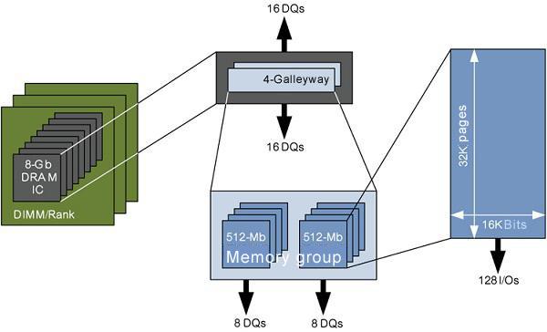
Picture 2:Typical DRAM architectures and hierarchies
A complete LPDDR4 memory chip consists of two high-level units: an array of memory and a DDR interface. Some parts of operations would affect memory arrays; The other part will affect the interface. The DDR interface can communicate with both memory arrays and external systems in the same time.
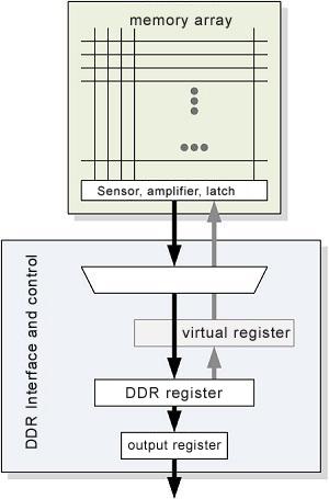
Picture 3:The logical structure of LPDDR4, memory arrays and DDR interfaces are divided in this picture. The arrows represent a single reading operation and write back
Figure 3 illustrates this relationship;namely, the DDR buffer acts as the main interface between the external system and the memory array. When the data is read, the array data is loaded into the DDR buffer at first. When carrying out writing operation, the required data is firstly written to the buffer from the external.
Because reading the contents of traditional DRAM array may destroy the original data, a write-back operation must be performed after each reading, which aims to restore the original value. After reading, the content of the DDR buffer is copied to the Shadow Register. When an external system reads the data from the DDR buffer, the Shadow Register is responsible for writing the data back to the selected page to restore the original value. Similarly, when writing data, the data of DDR buffer is transferred to the shadow register and then waits to be written; When carrying out writing operations, the DDR buffer can load new data.
Reading data of memory paging involves a series of activities, which is similar to two nested software DO loops. Each paging is divided into memory groups, which consists of 256 bytes and are read in batches. Therefore, there are 64 burst memory groups for a set of 16k-bit pages, and the full memory pages are read sequentially, which is similar to external DO loop.
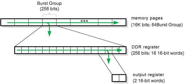
Picture 4:memory paging consists of memory groups, which are read in order; every batch of burst group is transferred to I/O by 16 continuous 16-bit.
Each burst transmission group is loaded into a 256-bit DDR buffer, which is divided into sixteen 16-bit words and read their contents sequentially, providing every 16-bit word for each frequency edge. This way of working is like that