
The physical structure of flash memory
Principles of flash memory devices
The previous article has already described the development history of solid state drives. Once the solid state drives used RAM as storage medium, currently most of them use flash memory chips as storage medium. DRAM solid state drives are rarely seen, mainly for special occasions. The first solid state drive in the world that was born in 1978 is based on DRAM. However, due to the volatility of power loss, of course cost, current solid state drives generally don’t use DRAM but flash memory such as NANA flash memory as storage medium. Many of the working principles of SSDs are based on flash memory. For example, the flash must be erased before written, that is, the write cannot be overwritten so that the solid state drive needs a garbage collection (or Recycle). When each block is erased for a certain number of times, the block either becomes a bad block or the data stored on it is unreliable. Thus, the SSD firmware must be wear-balanced. In other words, the data is written on all blocks on average instead of a few blocks, or the SSD will soon be scrapped. There are a lot of similar examples, for instance, many of the algorithms inside the SSD are for flash memory. Therefore, in order to break SSDs, flash memory will bear the brunt.
Flash memory is a kind of nonvolatile memory. That is, once power is off, data is not lost. The basic storage cell of flash memory is an NMOS-like bilayer floating gate MOS transistor, as shown in Figure 3-1.
![]()
Figure 3-1 The structure of floating gate transistor
The floating gate storing electrons is formed on a semiconductor with unidirectional current conduction between the source and drain. The floating gate is surrounded by an insulating layer, and the electrons stored in it aren’t lost due to power loss. So flash memory is called as nonvolatile memory.
The write operation is to add positive voltage to the control pole to enale electrons to enter the floating gate through the insulating layer. The erase operation is reversed by adding a positive voltage to the substrate to sink electrons from the floating gate, as shown in Figure 3-2.
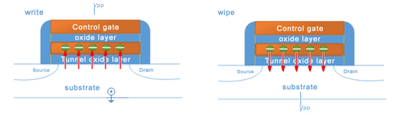
Figure 3-2 The left is the principle of write operation and the right is that of erase
At the Flash Memory Summit in 2014, Dr. Simon Sze, the inventor of the floating gate transistor, was awarded the Lifetime Achievement Award in recognition of his invention of the floating gate transistor. It is said that the invention of the floating gate transistor was inspired by this. One day, Simon Sze and his partner Dawon Kahng had lunch together in the company's canteen, and had cheese cakes for dessert. Looking at the sandwich cake, they are wondering what would happen if there was something in the middle of the MOS field effect transistor. Thus, the floating gate transistor was born. By some time in 2014, the number of floating gate transistors produced worldwide is 1,074,344,929,692,350,000,000.
This number is still growing. People feel that Simon Sze deserves a Nobel Prize, not just a lifetime achievement. After all, the discoverer of the giant magnetoresistance effect has won the Nobel Prize.
After the award, Simon Sze ordered a cheese cake for himself at the celebration party.
SLC,MLC,TLC
A storage cell stores a flash memory of 1-bit data,which we call SLC (Single Level Cell). Similarly, 2 bits are MLC (Multiple Level Cell), and 3 bits are TLC (Triple Level Cell). There are already vendors developing QLC, a storage cell that stores 4-bit data, which is not covered in this book.

Figure 3-3 The principles of SLC,MLC,TLC
As for SLC, a memory cell stores two states. When the electrons in the floating gate are more than a certain reference value, we sample it as 0. Otherwise, it is judged as 1.
Figure 3-4 shows the threshold voltage distribution function of the memory cells in the flash chip. The horizontal axis is the threshold voltage and the vertical axis is the number of memory cells. In fact, at 0 or 1, not all memory cells have the same threshold voltage, but a distribution centered on this voltage. When being read, the sampled voltage value falls within the range of 1 and is considered to be 1. When it falls within the range of 0, it is considered to be 0.
After erased, the flash reads a value of 1, and after charged, it is 0. Therefore, if you need to write 1, you don't have to do anyting. If you write 0, you need to charge.
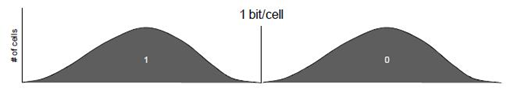
Figure 1-4 The threshold voltage distribution function of SLC
As for MLC, if a storage cell stores 4 states, it can only store 2 bits of data. In general, it is to divide the number of electrons in the floating gate. For example, when the electrons in the floating gate are less than 10, we sample it as 0. Similarly, 11 to 20 electrons is judged as 1, 21 to 30 as 2, more than 30 as 3.
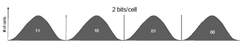
Figure 1-5 The threshold voltage distribution function of MLC
By analogy with TLC, if a memory cell stores 8 states, it can store 3 bits of data. It further divides the number of electrons in the floating gate on the basis of MLC.
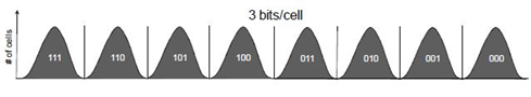
Figure 1-6 The threshold voltage distribution function of TLC
A memory cell of the same area, SLC, MLC, and TLC, can store 1, 2, and 3 bits of data, respectively, thus the capacity of flash memory becomes larger in turn in the DIE of the same area.
But at the same time, the more electronic division of a memory cell, the more delicate the number of electrons that are controlled to enter the floating gate during writing, so the longer the writing time will be. Similarly, reading requires trying to read at different reference voltages, to a certain extent, increasing the reading time. So we will see that in terms of performance, TLC is not as good as MLC, and MLC is not as good as SLC.
Table 3-1 shows an intuitive comparison of SLC, MLC and TLC in performance and Endurance.