
What is the value of an ASML lithography machine at price of $100 million? (2)
EUV:
The ultimate weapon of semiconductor industry Both TSMC and Intel are hoping that the most expensive "tool machine" in history can play an important role in 7nm process, which started trial production in 2017.
The global tens of billions of mobile phone wafers and memory every year is dependent on the cumbersome exposure and development process whose principle is similar to that of photographs for decades.
The most important and expensive one is the micro-projector which projects the circuit diagram. Over the past decade, the most advanced micro-projector in the world has used deep ultraviolet light with a wavelength of 193 nm. However, the most advanced transistors produced by Intel and TSMC have been small enough to be only tens of nanometers in size. This situation is just as the writing becomes smaller and smaller and finally the tip of the pen is thicker than the writing.
The EUV technology replacing superfine pen came from the "Star Wars Project" of the Reagan era in the United States, with only 13 nanometers of wavelength. According to Intel, the main promoter of the technology, EUV should be launched in 2005, but the production schedule has been delayed again and again.
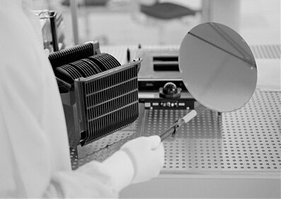
This technology is too difficult to implement. The energy and destructiveness of EUV light are extremely high. All parts and materials in the process challenge the limit of human technology. For example, air can interfere with EUV, so the production process has to be in a vacuum environment. Moreover, the mechanical action is accurate to the point where the error is measured in picoseconds. One of the most critical components, the mirror made by Zeiss, Germany, has to be flawless. The size of the defect can only be measured in Picometer.
This is an unbelievable matter! In an exclusive interview with World, Peter Wennink, president and CEO of ASML, explained that if the mirror is as large as Germany, the highest protrusion should not be higher than one centimeter. "Meeting these crazy requirements is our daily routine," said Peter Wennink, who took over as CEO two years ago. Because of the technical difficulty of EUV and the large amount of investment required, the other two major micro- projector equipment factories, Nikon and Canon in Japan, have abandoned development. ASML has become the last hope of semiconductor industry whether it can continue to sprint the next generation of advanced manufacturing process and develop more power-saving and faster transistors. "If we don't release EUV, Moore's law will be aborted," Peter Wennink said slowly. As a result, three years ago, there was an amazing deal that made ASML famous.
Intel, TSMC and Samsung have jointly invested 4.1 billion, 8.38 million and 5.03 million euros in ASML, respectively. (TSMC sold a 5% stake of ASML in May with a profit of TWD 21.4 billion) Peter Wennink explained that the major factories at that time required research and development of EUV to speed up. He told these customers, "If speeding up EUV research and development, we have to double our research and development expenditure."
As a result, ASML R&D funding has doubled to 1.3 billion euros per year, double than before. Therefore, ASML is responsible for half of the investment, and the three semiconductor giants account for the other half.