
What is the value of an ASML lithography machine at price of $100 million?
What kind of equipment can cost more than $100 million?
What is a lithography machine?
Lithography machine is one of the core equipment in chip manufacturing. It can be divided into several types according to its use: lithography machine for chip production, lithography machine for package, and projection lithography machine for LED manufacturing. The lithography machine used to produce chips is the largest shortcoming in semiconductor equipment manufacturing in China. The high-end lithography machine needed by Chinese wafer factories is totally dependent on imports. The lithography machine imported from the Netherlands by Xiamen enterprises is used for chip production.
In terms of high-end lithography machine, in addition to the faucet ASML, Nikon and Canon have also done lithography machine, moreover, Nikon has also received orders from Intel. But in recent years, Nikon, whose high-end lithography market is occupied by ASML, has been far behind ASML. Even if Nikon's latest AR-F immersion 630 sells at less than half of the average price of ASML Ar-F immersion in 1980D, it is still difficult to change this situation.
Why? On the one hand, after coming to power, Intel's new CEO stopped continuing his 620D contract with Nikon, which made Nikon lose a big customer. On the other hand, it is also related to Nikon's lack of technical strength. Nikon's lithography machine has many flaws compared with ASML. Nikon’s architecture in operating system is defective. What’s more, its actual performance is quite different from official propaganda. It’s impossible for large wafer factories such as TSMC, Intel, Samsung and GlobalFoundries to sell defective products in order to save a little money.
At present, Nikon's high-end lithography machine is basically defeated by ASML. There are only a few Nikon or Canon low-level and old lithography machines in the mainstream semiconductor production line. The rest are ASML lithography machines. In a way, Nikon's lithography machines can only grab the market at super-cheap prices. So how cheap is it?
According to data, ASML's EUV NXE 3350B is priced at over $100 million, and ArF Immersion is about $70 million. In contrast, the price of Nikon lithography machine is only one third of ASML.
Working principle of lithography machine
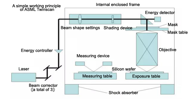
Measuring table and exposure table: A worktable for carrying silicon wafers.
Laser: That is the light source, one of the core equipment of lithography machine.
Beam corrector: Correct the incident direction of beam and make the laser beam as parallel as possible.
Energy controller: Control the energy eventually irradiated on the silicon wafer. Inadequate or excessive exposure will seriously affect the image quality.
Beam shape settings: Set the beam to different shapes, such as circle, ring, and so on. Different beam shapes have different optical characteristics.
Shading device: Prevent the beam from shining into the wafer when no exposure is required.
Energy detector: Detect whether the final incident energy of the beam meets the exposure requirements, and feedback it to the energy controller for adjustment.
Mask: A piece of glass engraved with circuit diagram at price of hundreds of thousands of dollars.
Mask table: A device that controls the motion of the mask. The accuracy of motion control is in the order of nm.
Objective: Compensate for optical errors and reduce the circuit diagram in equal proportion.
Silicon wafer: A wafer made of silicon crystals. There are various sizes of silicon wafers. The larger the size, the higher the yield. In addition, because the silicon wafer is round, it is necessary to cut a gap on the silicon wafer to confirm the coordinate system of silicon wafer. According to the shape of the gap, there are two kinds, called flat and notch.
Internal enclosed frame and shock absorber: Isolate worktable from external environment, keep balance, reduce external vibration interference, and maintain stable temperature and pressure.
In the process of chip fabrication, lithography machine transmits the light beam through the mask which draws the circuit diagram through a series of light source energy and shape control means, compensates various optical errors by objective, reduces the circuit diagram proportionally and maps it to the silicon wafer. And then, lithography machine develops the circuit diagram on the silicon wafer by chemical method. The general lithography process involves cleaning and drying silicon wafer surface, coating bottom, spin-coating photoresist, soft-baking, alignment exposure, post-baking, developing, hard-baking, laser-etching and other processes. After one lithography, the chip can continue to be coated and exposed. The more complex the chip, the more layers of the circuit diagram, the more precise exposure control process is required.