
ISSCC: Toshiba Memory uses PAM 4 to develop bridge chips, increasing SSD speed and capacity
According to China Storage, Toshiba Memory recently has announced that a developed bridge chip can provide solid state drives with high speed and large capacity.
Figure 1 Connection using a bridge chip
Compared with traditional bridge-free chip, the developed bridge chip with smaller area and lower power consumption can connect more flash chips and fewer high-speed signal lines. The results were presented at the 2019 International Solid-State Circuits Conference (ISSCC 2019) in San Francisco, California, on February 20.
In SSD, multiple flash chips are connected to controllers that manage their operations. As more and more flash chips are connected to the controller interface, the operating speed decreases, so the number of connectable chips is limited. In order to increase capacity, it is necessary to increase the number of interfaces. However, this further leads to a large number of high-speed signal lines connected to the controller, making it more difficult to implement wiring on the SSD board.
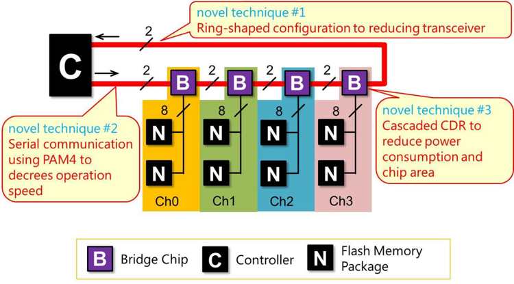
Figure 2 Improvement of bridge chip

Toshiba Memory overcomes this problem by developing bridging chip for connecting controllers and flash chips (Fig. 1). These three new technologies include ring-shaped configuration to reducing transceiver, serial communication using PAM4 to decrees operation speed and cascaded CDR to reduce power consumption and chip area. By using these technologies, the overhead of bridge chips is reduced, and a large number of flash chips can be operated at high speed using only a small number of high-speed signal lines (Figure 2).
The ring-shaped configuration of bridge chip and controller reduces the number of transceivers from two pairs to one pair, thus reducing the area of bridge chip. In addition, PAM 4 serial communication connecting the controller and the ring-shaped configuration of bridge chip can reduce the operating speed of the bridge chip circuit and relax its required performance. The CDR, which uses the characteristics of PAM 4 to improve jitter characteristics, eliminates the need for PLL circuits in bridge chips, contributing to smaller chip area and lower power consumption.
The prototype bridge chip is using 28nm CMOS process, and evaluates its performance by connecting four bridge chips and a controller in the daisy chain. Surprisingly, speed of all bridge chips and a controller is up to 25.6 Gb/s. Meanwhile, the BER error rate id less than 10-12.
In the future, Toshiba Memory will continue to develop bridge chip in order to further improve its performance with smaller chip area, lower power consumption, and larger capacity.