Explain the principle and use of NAND Flash with examples (3)
12. Programming operations
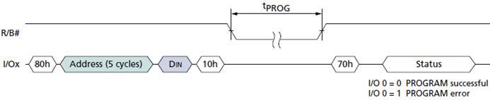
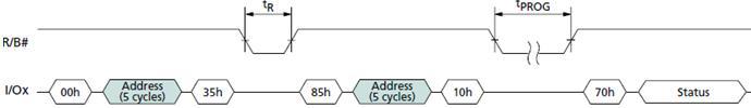
PROGRAM PAGE 0x80-0x10:
Micron NAND Flash only supports page programming. Within a block, the page must be programmed continuously from the lowest bit of a block’s page to the highest bit, prohibiting the programming of random page addresses.
The chip also supports partial programming of the page, which means that any single bit can be programmed only once before an erase is required. However, such pages can be divided into up to 8 programming operations before an erase.
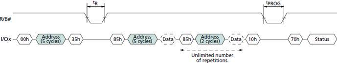
SERIAL DATA INPUT 0x80:
PAGE PROGRAM operation requires loading SERAIL DATA INPUT(0x80) command before entering into the command register. With 5 address cycles, the serial data is loaded into a worthwhile starting address through a continuous WE# cycle. PROGRAM (0x10) commands are written after data input is completed. The internal write state cycle automatically executes the appropriate programming algorithm, and controls all necessary timing programming and comparison operations. Write comparisons only detects whether "1" has been successfully programmed as "0".
R/B# is low during array programming (tPROG). During programming operations, only RREAD STATUS and RESET commands are valid. Bit6 of status register reflects the status of R/B#. When the chip is ready, the status of reading Bit0 determines whether the programming operation succeeds or fails. The command register stays in reading status register mode until a new valid command is written.
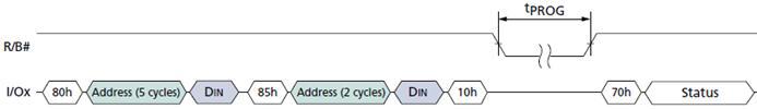
RANDOM DATA INPUT 0x85:
After dataset input is initiated, data can be written to the new column address via RANDOM DATA INPUT command. Before issuing the 0x10 command, you can use the 0x85 command multiple times on the same page.
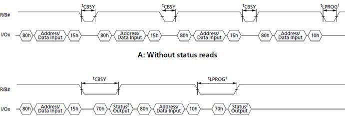
PROGRAM PAGE CACHE MODE 0x80-0x15:
CACHE programming is actually a buffer programming mode of standard page programming commands. Programming begins with the release of SERIAL DATA INPUT (0x80) command, followed by five address cycles and all or part of the page's data. Data is copied to the CACHE register, and then releasing CACHE WRITE (0x15) command. Data is latched to the data register along the rising edge of WE#. During this latch period, R/B# is low. After the end of the latch, R/B# becomes higher and programming begins.
When R/B# is higher, new data can be written by publishing another CACHE PROGRAM command. When R/B# remains low, it is controlled by the actual programming time. The first time is equal to the time it takes for data to be written from CACHE register to the data register. After that, only after the contents of the data register are programmed into the array can the cache register be locked into the data register. Later R/B# being lower should be longer in practice.
Bit6 in the status register that reflects CACHE R/B# can be read out through the READ STATUS command to determine when the cache register is ready to accept the new data.
Bit5 in the status register that reflects R/B# can be queried to determine when the actual array programming of the current programming cycle is completed.
If only R/B# is used to determine whether the programming is completed, then the last page of the programming sequence must use PROGRAM PAGE (0x10) instead of CACHE PROGRAM (0x15). If the CACHE PROGRAM command is used every time, Bit5 of the status register must be used to determine whether the programming is over.
When Bit6 of the status register is 1, Bit0 of the status register returns to the previous page to determine whether the programming is successful or not. The successful or not status of the current PROGRAM operation depends on Bit0 status when Bit5 is "1" (ready status).
13. Internal data move
Internal data move requires two command sequences, first publishing a READ FOR INTERNAL DATA MOVE(0x00-0x35), and then releasing a INTERNAL DATA MOVE(0x85-0x10) command. However, data relocation only supports the die range of read data.
READ FOR DATA MOVE 0x00-0x35:Firstly write 00 to the command register, and then the internal source address (5 cycles), followed by 0x35, which will start to transfer one page from memory to the CACHE register. Although the addresses of 5 cycles are published, column addresses are ignored. The chip is now ready to accept INTERNAL DATA MOVE(0x85-0x00) command.
INTERNAL DATA MOVE 0x85-0x10: After READ FOR INTERNAL DATA MOVE command is released and R/B# becomes higher, INTERNAL DATA MOVE command can be issued, which can transfer the contents of CACEH register to data register and then programs to the new target address. With the emerge of INTERNAL DATA MOVE command and the address sequence, R/B# becomes lower, while the internal control logic automatically programs data to a new page. READ STATUS command and Bit6 of status register can replace R/B# to determine when the programming is completed. The Bit0 of status register indicates whether the operation was successful. During INTERNAL DATA MOVE command, RANDOM DATA INPUT(0x85) is used to modify one or more words of the original data: First, use the 0x00-0x35 command sequence to copy data to the CACHE register. Second, use RANDOM DATA INTPUT(0x85) command with the data address to be modified to make new data input presented at the external data foot, which will copy new data to CACHE register. When 0x10 is written to the command register, original data and modified data are transferred to the data register. A new page of programming will begin. If necessary, RANDOM DATA INPUT command can be issued several times before starting the programming sequence(0x10).Because INTERNAL DATA MOVE operation does not use external memory, ECC cannot be used to check for errors before programming, which may cause data errors. In this case, multiple INTERNAL DATA MOVE operations performed contributes to accumulating these bit errors without corrections. For this reason, we strongly recommend using robust ECC scheme in INTERNAL DATA MOVE system, resulting in correcting two or more errors for every SECTOR.