
Explain the principle and use of NAND Flash with examples (4)
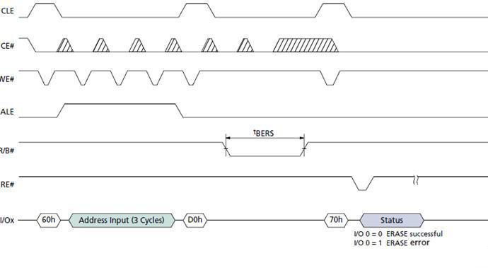
14. Block erasure operation, 0x60-0xD0
Erase one block at a time. The address A[28:18] of three cycles is required to publish ERASE SETUP(0x60) command first, then three address cycles, followed by ERASE CONFIRM(0xD0) command. The status of erase operation can be read by READ STATUS RESGISTER command. when Bit6=1, the operation is completed. Bit0 indicates the pass or failure condition, 0 meaning pass.
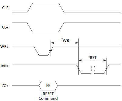
15. Reset operation, 0xFF
The reset operation allows the chip to enter a known state, interrupting the command sequences being processed. For example, RANDOM READ, PROGRAM, and ERASE commands can be interrupted in a busy-state chip. The location being programmed or the contents of block being erased become invalid, while data may be erased or programmed partially. The command register is cleared and ready for next command.
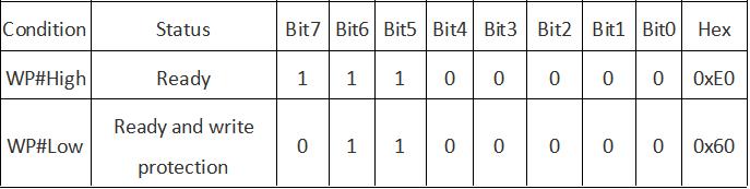
Contents of status register after reset:
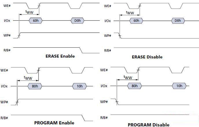
16. Write protection operations
Write protection is designed to prevent careless programming and erasure operations. When WP# is low, all programming and erasure operations are prohibited.
17. Error management
All blocks of Micron NAND chips are not guaranteed to be good when they are manufactured. As long as there are not less than 2008 intact pieces among 2048 chips, they are considered qualified products to be manufactured. But the existence of bad blocks does not affect the operation of good blocks. In the application system, the algorithms of bad block progection, substitution and error correction should be provided to ensure the high reliability and integrity of the data.
The first block of each CE# (physical block address is 0) is absolutely tested and intact. This provides a storage location for BOOT code and important information.
Before the chip is manufactured, the manufacturer will use non-0xFF programming to identify the bad block at the first backup location (column address is 2048) on the first or second page of each bad block.
The system software should check the first backup address data on the first or second page of each block before performing any erasure or programming operations. This creates a bad block table.
After a certain period of time, some locations of memory may not be programmed and erased correctly. In order to ensure the reliability of data, some precautions should be taken, such as:
Always check status after a write, erase, or data move operation.
Use some types of error detection and correction algorithms to recover some minor iede1 errors.
Use bad block substitution algorithm.