
How to exploit IO performance of NAND Flash
NAND Flash chip is the basic storage unit of SSD. The development and structural changes of NAND Flash chip will promote the rapid development of the entire flash memory industry. When designing a flash memory system, especially when designing a NAND Flash controller, SSD disk, or SSD card, we need to have a thorough understanding in operation, interface commands, and timing of NAND Flash. Although a NAND Flash chip is very small due to the packaged form of LGA or TSOP, its internal structure is still very comPlex. In particular, as storage density continues to improve, there are more and more abstract concepts in NAND Flash, such as Flash particles, Device, Die, Plane, block, and page. Flash particles are the basic packaging particles of chip; each particle can encapsulate multiple devices, and each device can be consider as a separate chip with independent control and data signal lines. Each device can be made up of multiple Dies. There are independent operation registers, status indication signals and external signal lines shared within Dies. A die can be divided into multiple Planes, each of which has a independent data register group that can perform concurrent operations on multiple Planes under certain circumstances. A Plane is composed of several Blocks, each of which is a separate data Block erasure unit. A Block is finally split into many Pages, each of which is the basic unit of reading and writing operations.
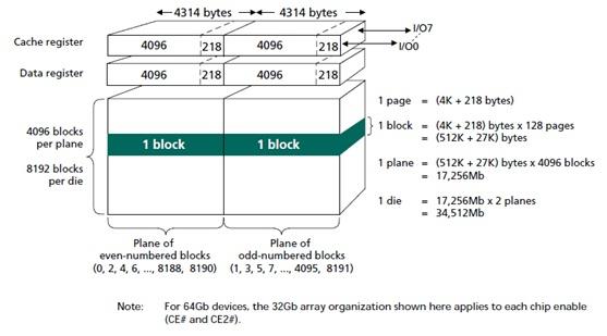
Taking Micron Flash chip as an example, MT29F32G chip consists of one Die that includes two Planes. MT29F64G chip consists of two Dies, both of which belong to two Devices, respectively. One Die is made up of two Planes. The basic unit structure of Die for MT29F32G and MT29F64G chips can be described as follows:
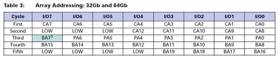
The address information of the MT29F32G and MT29F64G chips can be defined in the following table.
Due to the increased storage density, MT29F128G chip consists of two Devices. Each of Devices includes two Dies, each of which contains two Planes. The structure of the basic storage unit Device in the MT29F128G chip is described as follows:

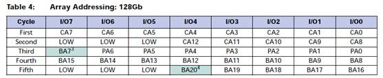
The address information of the MT29F32G and MT29F64G chips can be defined in the following table.
After understanding the internal structure of NAND Flash, we need to think about how to take advantage of the internal structure of NAND Flash from the software level to improve overall IO performance.
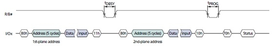
A Plane has independent data registers and can we concurrently operate Plane to improve IO performance? Taking Micron MT29F128G chip as an example, each Die can be divided into two physical Planes, each of which consists of a 4314-byte data register, a 4314-byte Cache register and a 4K-Page Block Array. Because the data registers of two Planes are physically independent, these two Planes can perform Program, Read, and Erase operations simultaneously to improve the system IO performance of NAND Flash. The timing diagram of two Planes reading data at the same time is as follows:
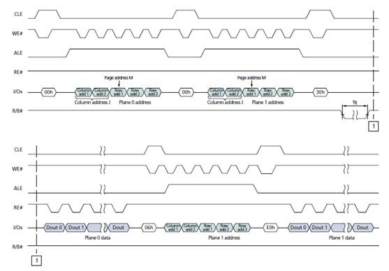
As can be seen from the timing diagram above, the concurrent operation between two Planes is not so arbitrary. When you need to read data from both Planes at the same time, load the address information for the first Plane, and then the second Plane. When both address information are loaded, issue the end command 30H. The entire Die is busy without being affected by any manipulation, while R/B# signal is low. At this busy state, the data is loaded from NAND Flash into two Planes registers. After R/B# signal is restored, the data in two Planes can be read. It is noteworthy that data read in the second Plane requires the support of the 06H-E0H command. From this point of view, because two Planes have only independent data register but shares the operation register, they cannot be very good to do very arbitrary data concurrency.
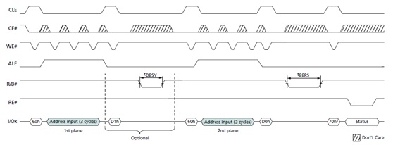
The timing of concurrent write operations of two Planes is shown in the following figure:
Similar to concurrent read operations, concurrent write between two Planes is not arbitrary and requires same operation at the same time. The concurrent operation of two Planes requires a command to be initiated at the same time. For write operations, you first need to load access addresses of two Planes. The terminator 11H of the first address does not trigger a real programming operation, while the terminator 10H of the second will actually trigger the programming operation. Once the programming operation is started, the status signal R/B# is low. After the programming operation is complete, the status signal can be restored.
The timing of concurrent erasure operation of two Planes is shown in the following figure:
Similar to concurrent read and write operations, concurrent erasure operations of two Planes requires loading both address information at the same time, and then performs erasure operation. Compared with serial operations, concurrent operations can improve the overall performance of NAND Flash.
Therefore, from the above description, although data registers between t two Planes are completely independent, operation registers are shared, allowing read-write and erase operations to be performed concurrently on them. However, the condition for this concurrent operation is that two Planes must perform the same operation at the same time, instead of executing different operations at will, independently, and concurrently, which is the limitation of concurrent operations for two Planes. But even so, if the software can be designed good algorithms that fully enable multiple Planes to execute concurrently, IO performance can be greatly improved.
A truly independent concurrent unit in NAND Flash chip is Die. Taking MT29F128G as an example, there are two Dies inside a Device. Both of Dies have independent operating registers and status signal lines, but share external control and status signal lines. In this case, the chip provides an interleave mode of operation, which can complete concurrently the read-write and erase operations of two Dies. The following is a concurrent reading timing diagram of two Dies:
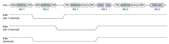
As can be seen from the figure above, two Dies have independent R/B# signal lines. The external status signal lines are the logic and result of internal status signal. The two Dies can operate independently and concurrently. Because they share external interfaces, they need to be serialized in data output.
The concurrent write timing of Interleave is shown in the following figure:
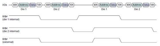
Similar to concurrent read operations, two Dies can perform write operations concurrently.
This concurrent operation is more casual at the Device level. Different Devices have completely independent external interfaces, so two Devices can perform independent operations at the same time.
In summary, there are 3 kinds of concurrent execution units in NAND Flash chip, namely Device, Die, and Plane. Due to independent data registers, multiple Planes can perform the same operation concurrently; Die has a independent operating register, an independent internal status signal line, and a shared external interface, so multiple Dies can be operated independently or concurrently. There are independent control and signal lines between Devices, so multiple Device can be concurrent at will. Making good use of these concurrent units inside NAND Flash chip can greatly improve IO performance of flash memory.