
Self-assembly Technology-The New Direction of Chip Manufacturing(1)
Moore's law is well known in the field of semiconductors. The semiconductor industry has developed rapidly promoted by Moore's law in the past few decades. As the size of transistors approaches the physical limit, semiconductor processes are becoming increasingly difficult to advance.The sound that Moore's law is invalid begins to spread. However, the scientific community hopes that find some new technology to promote Moore's law.

Is Moore's law dead?
Moore's law was put forward by Gordon Moore who is co-founder of Intel in half a century ago, which explain that the number of transistor integrated circuits containing doubles about every 18 to 24 months when the price doesn't change.
utThe semiconductor industry has been advancing rapidly according to Moore's law since it put forward.However,Moore's law began to slow down and its economic benefits have also begun to decline after 28nm technology.
Although TSMC has mass product 7nm technology in the first half of last year and 5nm technology is on the way, there may still be a long way to go for 3nm or even 1nm ,which is undoubtedly more difficult.
What is pessimistic is that the density of transistors can increase further as the process improves while the performance gains or power consumption reduction are less and less. For example, the area of transistor is reduced by 40% and the speed is increased by 30-40% from 28nm to 16nm.But if the speed is increased, the power consumption will not be reduced much. Prior to 28nm, the power consumption, area and speed of each generation of process upgrading can be reduced by more than half in each generation process technology upgrade.But now that good thing is over.
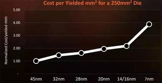
Besides, as the process continues to evolve from 10nm to 7nm, 5nm, 3nm and 1nm, the cost becomes more expensive. The economic benefit that performance doubles or more every two years at the same price will be no longer in existence, which produced by Moore's law.
Semiengingeering previously published an article on the process and chip development costs. It is pointed out that the chip development cost of 28nm node is $51.3 million. A 16-nm node chip costs $100m; The 7nm node chip costs $297 million; The 5nm node chip will cost $542 million to develop. Since 3nm is still in early stages of development, its development costs are still uncertain and it could cost more than $1 billion.
What is more, advanced fabs also require a lot of cash to upgrade processes with the latest equipment, which will drive up the cost of chips. For example,5nm need to use the latest EUV extreme ultraviolet lithography technology. While only ASML supply EUV lithography in the world, which the price of is up to $100million.
Obviously, with the process technology approaching the physical limit, not only is the technology more difficult to implement and is the required equipment more complex, but the cost of developing chips is also increasing rapidly. If the chip manufacturers do not have enough strength and chip shipments, they will be difficult to bear high costs.
New "self-assembly" technology
Under the circumstance that the promotion of "Moore's law" is more and more difficult, numerous semiconductor enterprises including Intel hope to promote the economic benefits of Moore's law through "kernel architecture innovation" (such as using non-von neumann system architecture), chip technology transformation from the original 2D to 2.5d /3D stack, spintronic, neuronal computing, quantum computing and other methods.
These new technologies may be more or less familiar to you.In the TED talk held in Germany last year, American researchers Karl Skjonnemand propose a new idea that "Molecular engineering and natural simulation methods" can be used to realize self-directed assembly of transistors, which can greatly reduce the cost of semiconductor manufacturing.

Karl Skjonnemand is currently the technical director of a US company focused on advanced nanometer materials for future chip manufacturing development. He has 20 years of project management experience in Asia Pacific, Europe and the US.
So what are the advantages of so-called "self-assembling" transistors compared with traditional semiconductor manufacturing process?
Karl Skjonnemand thinks many microstructural characteristics of transistors in traditional chips are repetitive, which is a highly periodic . So, he want to take advantage of this periodicity in alternative technologies.He build transistor by self-assembling material and naturally formed periodic structures, which produce fine pattern rather than trying to make breakthroughs in pattern projection techniques that have become increasingly difficult.

The principle of self-assembly is seen everywhere in nature.For example, that our lipid membranes, cell structures,DNA replicate and passed down from generation to generation is a natural assembly technique. Therefore,Karl Skjonnemand think self-assembly technology can be applied to chip manufacturing.
He introduced a technique self-assembly materials (a kind of organic semiconductor) called "block copolymer"-consisted of two polymer chains that are only a few tens of nanometers long, but they repel each other. They can be compulsively combined together to create an "embedded frustration" in the system. A small piece of material can contain billions of such polymer chains, where similar compounds stick together and mutually exclusive ones separate. These compounds move around until they form a specific shape.
Karl Skjonnemand suggested that natural self-assembly shapes are nano-sized, regular, periodic and very long, which is what we need in transistor arrays.Importantly, they can provide finer details than conventional transistor etching.
Therefore, we can use molecular engineering to design different sizes, different shapes and different shapes periodically.For example, if we choose a symmetrical molecule whose two polymer chains are similar in length, the natural self-assembling structure is a long curved shape, like a fingerprint, whose width and spacing depend not only on the length of the polymer chain, but also on the level of frustration within the system.
We can also create more complex structures, if we use asymmetric molecules, one of which is significantly shorter than the other. In this case, the short chain forms a solid ball in the middle encased in a longer mutually exclusive polymer chain to form a natural cylinder. It is depends on the length of the polymer chain and the level of the embedded frustration that size of the cylinder and the distance and periodicity between the cylinders. 
Related Articles:
The development of Moore's Law from the perspective of 8-year ...
OSAT has become a breakthrough of Chinese semiconductor industry
TSMC, Intel and Samsung are still cooperate with ASML to speed up ...