
Types and Comparative Analysis of NAND Flash
As a common memory chip, NAND Flash is widely used, especially, in the consumer electronics products. Thus, the memory density is improved while the cost of NAND Flash is more and more sensitive. Because the cost depends on the chip area, Flash will be more cost effective if storing more data in the same area.
There are three types of NAND Flash , including Single Level Cell(SLC),Multi Level Cell(MLC)and Triple Level Cell(TLC). TLC Flash can store more data in the same area than MLC while MLC can store more data than SLC. Another type of NAND Flash is called as 3D NAND which achieves greater density by vertically stacking multiple layers of memory cells on the same wafer.
SLC Flash
In SLC Flash, each of memory cell can only store one bit of information. The threshold voltage of a logical 0 or logical 1 cell is compared to a single voltage level. If the voltage is higher than the level, the bit is considered logical 0. If not, logic 1.
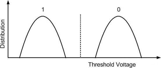
Picture 1: the voltage in the SLC Flash cell is compared with the threshold voltage to determine whether it is logical 0 (above the threshold) or logical 1 (below the threshold).
Owing to only two levels, so the voltage margin between the two levels can be very high. This makes cell reading easier and quicker. And, RBER is also low. Because of large voltage margin, the impact of leakage and interference is small during read operations. Low RBER also reduces the number of ECC digits required for a given block of data.
Another advantage of a large voltage margin is that the wear effect is relatively small. Because tiny charge leaks has a relatively low impact. A wider distribution of each logic level helps to program or erase the cell at a lower voltage, which further increases the durability of the cell and increases the lifetime, the number of P/E cycles.
At the same time, a disadvantage of large voltage margin is that the cost of each cell is higher compared with other types of Flash which can storage more data in the same area. SLC flash is typically used in cost-insensitive applications that require high reliability and durability, such as industrial and enterprise applications that require a large number of P/E cycles.
MLC flash memory
In MLC Flash, each memory cell can storage two-bits of information, namely 00, 01, 10 and 11. Under this circumstance, the threshold voltage is compared to three levels (total of 4 voltage bands).
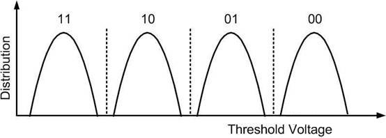
Picture2: the voltage in the MLC Flash cell is compared with three threshold voltage to determine two-bit values.
With more levels of comparison, the reading operations of MLC flash needs to be more precise. Compared with SLC Flash, the reading speed of MLC flash is slower. Owing to low voltage margin, RBER will be high and more ECC bits are required for a given block of data. Now, the effect of wear is obvious because any voltage leakages can generate more impact compared with SLC flash, thus reducing the lifetimes (the number of P/E cycles).
Programming is also much slower because of the careful programming required to store the charge in the tight window required for each logic level. Its main advantage is lower cost per bit, 2~4 times lower than SLC Flash. MLC Flash is usually used for more cost-sensitive applications, such as consumer electronics or gaming systems, where performance, reliability, and durability are less critical, and where P/E cycles are relatively low.
eMLC Flash
Although low cost of MLC Flash is a driving factor, low reliability and durability is not suitable for enterprises. In order to exert its advantages of low cost, flash manufacturers have created an optimized MLC flash with higher reliability and durability, called eMLC. The data density of it is usually low in order to provide better voltage margin for improving reliability. Its slower erase and program cycles are often used to reduce the effects of wear and increase durability. There are many other technologies that can improve the reliability and durability of eMLC, which work differently depending on the manufacturer.
TLC Flash
In TLC Flash, each memory cell stores 3 bits of information. The threshold voltage is now compared to 7 levels (a total of 8 voltage bands).
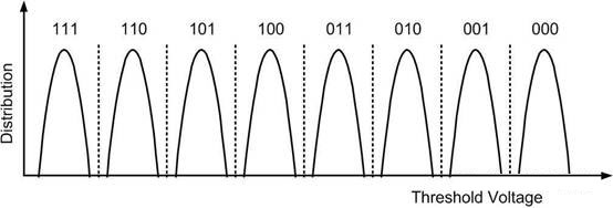
Picture 3: The voltage in the TLC flash cell is compared with seven threshold voltages to determine its logical three-bit values.
Compared with SLC Flash, the reading operations of TLC need to be more precise and slow. RBER is also high, increasing the need for more ECC bits for a given block of data. The effects of wear are also magnified, significantly reducing the lifetimes (P / E cycle times).The programming operation is also slower because the voltage needs to store the charge within the window required for each logic level accurately.
The advantage of TLC is that its lowest cost is much lower than that of SLC Flash and MLC Flash. TLC Flash is usually used for cost-sensitive applications with less demand for P/E cycles, such as consumer applications.
Comparison of SLC, MLC, eMLC and TLC
Picture 1 gives a comparison of the main parameters of different types of flash memory assuming a similar lithography process. These values are only indicative of comparative performance and may be inaccurate for a particular memory product.
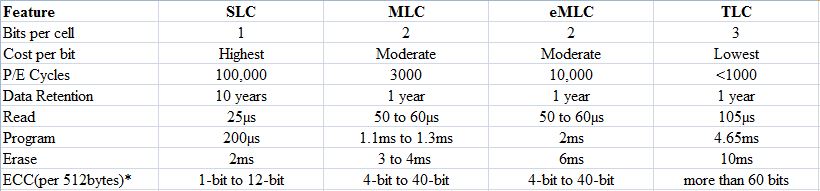
Picture 1 gives a comparison of the main parameters of different types of flash memory.
* The number of ECC bits depends on the process node; smaller process nodes require more ECC bits.
3D NAND Flash
All of the different flash memories discussed above are two-dimensional, which means that the memory cells are located only in the XY plane of the chip. With 2D flash memory, the only way to achieve higher density in the same wafer is to shrink the process nodes. The disadvantage is that errors in NAND flash are more frequent for smaller nodes. In addition, there are limitations on the minimum process node that can be used.
In order to improve storage density, manufacturers have developed 3D NAND or V-NAND (vertical NAND) technology, which stacks storage cells in the Z plane onto a single wafer. Building in this way helps achieve high density for the same chip region. In 3D NAND flash, memory units are connected as vertical strings rather than horizontal strings in 2D NAND.
The advantage of 3D flash is that there are significantly more storage locations in the same area. This also allows manufacturers to make more reliable flash memory using larger process nodes.
Another major technological shift in 3D Flash is the use of charge-trap Flash rather than floating gate transistors. The charge trap is structurally similar to FGMOS, except that the floating gate is replaced by silicon nitride film. Note that charge traps are not widely used in the market due to the difficulty of large-scale manufacturing. Charge-trap technology has been used for 3D flash memory because of the difficulty of manufacturing vertical strings of floating gate transistors and other inherent advantages of charge-trap technology.
Compared with FGMOS, charge-trap memory has many advantages. The charge trap based memory can be programmed and erased at lower voltages for improved durability. Since the trap layer (nitride) is an insulating layer, charges are not leaked, thereby improving reliability. Since the charge does not flow from one side of the charge well to the other side, more than one bit of charge can be stored in the same well layer.
The trend of future
All major flash memory manufacturers are actively working on different ways to reduce the cost per bit of flash memory while actively increasing the number of vertical layers in 3D NAND Flash. Although 15nm seems to be the smallest successful node in NAND flash, the shrinking of Flash's lithography nodes continues. The combination of MLC and TLC technology with 3D NAND flash memory is also being actively explored, and many manufacturers have seen the dawn of success. With the advent of new technologies, we may soon see that memory cells can store one byte of data and vertical layers, up to 256 layers, or even higher.
Relaed Articles:
How to exploit IO performance of NAND Flash
What is TLC granule? What is the difference between it and MLC and ...
The comparison between SLC, MLC and TLC - Memory Storage