
What is on earth the difference between NAND Flash and NOR Flash? (1)
When choosing a flash memory, embedded system designers must consider many factors: which type of flash architecture to use, whether to choose a serial or parallel interface, whether to require a checksum code (ECC) and so on. If the processor or controller supports only one type of interface, options are limited. Therefore, it is easy to select a flash memory. However, this is often not the case. For example, some FPGAs support serial NOR flash memory, parallel NOR flash memory and NAND flash memory to store configuration data, as well as they can be used to store user data, which makes it is more difficult to select the correct memory device. This article will discuss different aspects of flash memories, focusing on the differences between NOR flash memory and NAND flash memory.
Storage Architecture
A flash memory stores information in memory cells made of floating-gate transistors. The names of these techniques explain how memory cells are organized. In NOR flash memory, one end of each memory cell is connected to the source line and the other end is directly connected to a bit line similar to NOR gate. In NAND flash memory, several memory units (usually eight) are connected in series similar to NAND gates (see Figure 1).
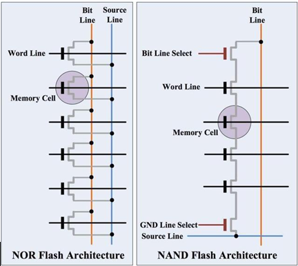
Figure 1: NOR Flash (left) has architecture similar to NOR gates. Similarly, NAND Flash (right) is similar to NAND gates.
NOR flash architecture provides enough address lines to map the entire memory range, which provides the advantages of random access and short read time, making it an ideal choice for code execution. Another advantage of is 100% known component life. While disadvantages are higher cost per bit and slower write and erase speeds due to the larger cell size.
In contrast, NAND flash memory has smaller cell sizes and higher write and erase speeds than NOR flash memory. Disadvantages of NAND are slower read speed and I / O mapping type or indirect interfaces, which are more complex and do not allow random access. It is worth noting that the code execution in NAND flash is achieved by mapping the content to RAM, which is different from executing code directly from NOR flash. Another major drawback is the existence of bad blocks. NAND flash usually has 98% good bits when additional bit failures occur throughout the whole life cycle of the component, so the ECC function is required within the device.
Memory Capacity
NAND flash is much denser than NOR flash, mainly because of its lower cost per bit. NAND flash usually has a capacity of 1GB to 16GB. The density of NOR flash ranges from 64MB to 2GB. Due to the higher density of NAND flash, it is mainly used for data storage applications.
Erasing / Reading & Writing
Memory is organized into erase blocks in NOR and NAND flash memory, which helps maintain performance while keeping low costs. For example, smaller block sizes can achieve faster erase cycles. However, the disadvantage of smaller blocks is the increases in chip areas and memory costs. Because of the lower cost per bit, NAND flash memory can support smaller erase blocks more economically and efficiently than NOR flash memory. At present, the typical block size of NAND flash is 8KB to 32KBand that of NOR flash is 64KB to 256KB.
The erase operation in NAND flash memory is very simple. While in NOR flash, each byte needs to be written "0" before being erased, which makes the erase operation of NOR flash much slower than that of NAND flash. For example, it takes 3.5ms for NAND flash S34ML04G2 to erase 128KB blocks while NOR flash S70GL02GT requires about 520ms to erase similar 128KB sectors. The difference is nearly 150 times.
As mentioned previously, NOR flash memory has enough addresses and data lines to map the entire storage area similar to the way SRAM works. For example, a 2GB (256MB) NOR flash memory with a 16-bit data bus will have 27 address lines for random read access to any memory location. In NAND flash, the memory is accessed by a multiplexed address and data bus. Typical NAND flash memory uses 8 or 16-bit multiplexed address / data bus and other signals, such as chip enabling, write enabling, read enabling, address latch enabling, command latch enabling and ready / busy. NAND flash needs to provide commands (read, write or erase) then address and data. These additional operations make the random read speed of NAND flash much slower. For example, NAND flash S34ML04G2 needs 30μS. While NOR flash S70GL02GT requires 120nS. Therefore, NOR type is 250 times faster than NAND type.
Related Articles:
How to exploit IO performance of NAND Flash
Explain the principle and use of NAND Flash with examples (1)
Comparison of NorFlash, NandFlash and eMMC (1)