
This carbon nanotubes +RRAM+ILV 3DIC wafer may change the semiconductor industry
Max Shulaker, an assistant professor at the Massachusetts Institute of Technology, recently presented a 3DIC wafer stacked with carbon nanotubes and RRAM stacked through ILV technology at the DARPA Electronic Revival Initiative (ERI) Summit. The wafer indicates special significance that it is the first time that the carbon nanotubes and RRAM and ILV 3DIC technology have been officially processed by a third-party foundry, SkyWater Technology. That represents the carbon nanotubes and RRAM and ILV 3DIC technology officially move to commercialization and large-scale applications from school Labs.

The origin of Carbon nanotubes, RRAM, ILV 3DIC
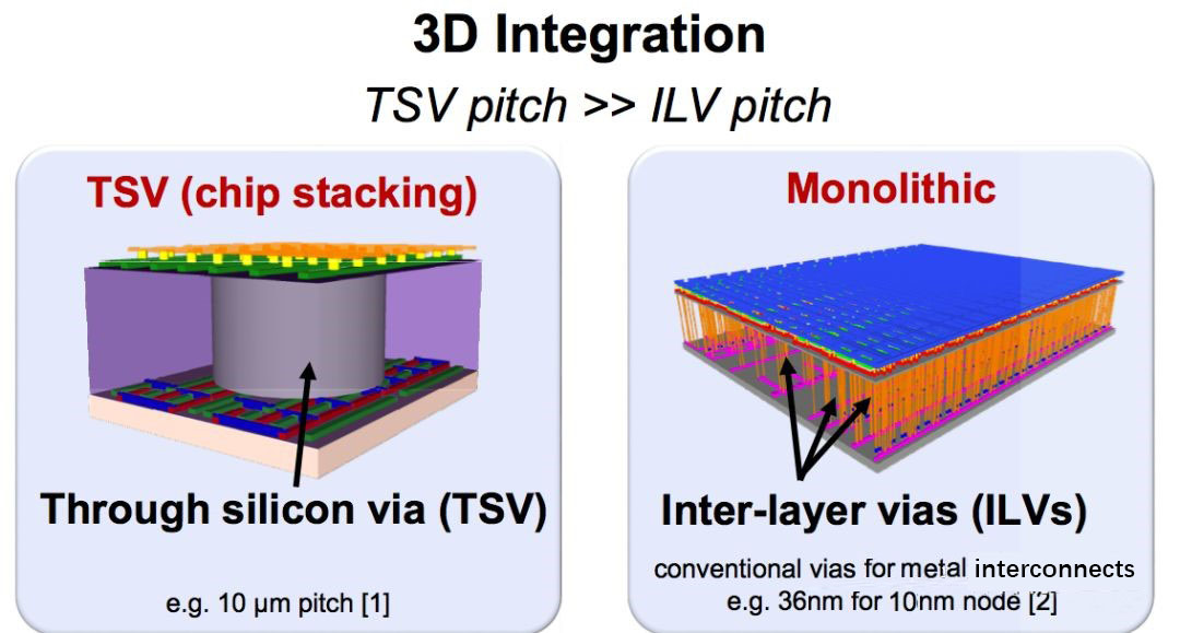
Let’s start with 3DIC technology. As the Moore's law is generally closed to the bottleneck, it is more and more difficult to increase the chip performance by semiconductor process reducing. To solve this problem, semiconductor industry puts forward a way, which is to combine the advanced packaging with heterogeneous computing, to continually improve chip system performance. Traditional generic chips try to solve all application problems with a single common processor, so it's hard to meet the needs of applications as Moore's Law approaches failure and processor performance go slow today. In the high-level package with heterogeneous computing paradigm, multiple chips are tightly integrated in one package, each chip is tailored for specialized applications, so can handle efficiently applications and meet the needs of the application scenarios. 3DIC is one of advanced packaging technologies. 3DIC pile several chips together and can achieve the high-speed data communication through TSV technology. When using 3DIC, the distance among the chips are quite near and the density of Internet line is so high that can achieve the high-speed signal transmission. So, packaging the processor chip and memory chip together can achieve high speed interconnections between processors and memory, and then solve the problems of memory access bottleneck (memory wall) to increase the overall performance of the chip system.
Through the above analysis, we can see the key of 3DIC is how to achieve the interconnection among high-density chips, which is also the protagonist of this article—the key breakthrough of the carbon nano tube + RRAM + ILV 3DIC technology. In the traditional TSV 3DIC, different chips are piled together and interconnected through TSV technology with the distance among the interconnection line of about 10 microns. Compared to TSV 3DIC , carbon nano tube +RRAM +ILV 3DIC does not produce multiple chips and stack them in packages. It directly achieves that several chips (single 3DIC) on one wafer. How does it achieve? As we know, the fabrication process of traditional chips is to make active area firstly, and then make multilayer metal interconnection on the active area. Each time a layer of metal interconnect is completed, an insulated interlayer dielectric layer (inter-layer dielectric, ILD) is deposited above it. And then the metal interconnect layer is re-grown above the ILD layer. The process goes on until more than a dozen layers of metal interconnection are completed. At the same time, the interconnection of different metal layers can be achieved through inter-layer through holes (inter-layer via, ILV).
The achievement way of the carbon nano tube +RRAM+ILV is a little bit similar as the producing way of making metal interconnection on the traditional chips: After finishing the underlying standards CMOS active area, it is not only to make the metal interconnection on it, but also has the carbon nano tube and RRAM. For example, Max Shulaker has achieved the NMOS active area->ILD+ILV-> carbon nano tube layer->ILD+ILV->RRAM->ILD+ILV-> carbon nano tube layer in 2007. Then it could achieve several wafer tube pile 3DIC on one wafer without any packaging technique. What is more important that interconnection density of 3DIC is extremely high through ILV technology, thus improving the performance of the overall chip system.
Why are the carbon nano tube and RRAM used? The reason is not only that carbon nano tube and RRAM can surpass the traditional CMOS wafer tube/Flash memory performance and efficiency ratio, but also the temperature of ILV technology must lower than 400 degree, or it will damage the logic of other layers. But carbon nano tube and RRAM can accept the lower temperature technology, then it can be a perfect combination with LIV; instead, the temperature of traditional silicon CMOS technology is more than 1000 degree, it is only can be the bottom layer of 3DIC.
The latest release at DARPA ERI summit meeting
Max Shulaker, an assistant professor at the Massachusetts Institute of Technology, received warm applause from the audience when he presented the carbon nanotubes +RRAM+ILV 3DIC wafers at the DARPA ERI Summit this week. As mentioned above, Shulaker has completed production of carbon nanotubes +RRAM+ILV 3DIC in the lab's foundry and published the paper in Nature in 2017. The carbon nanotubes +RRAM+ILV 3DIC wafer was prepared successfully for the first time in a third party, SkyWater Technology.
Currently, carbon nanotubes +RRAM+ILV 3DIC was produced by 90-nanometer process, which is expected to achieve a smaller feature size and higher performance in the future. In addition, SkyWater will provide PDK after the process yield reaches the mass production standard. Based on this, Skywater will be able to build businesses about the carbon nanotubes +RRAM+ILV 3DIC process and license the technology to other OEM factories.
Will carbon nanotubes +RRAM+ILV 3DIC change the semiconductor industry?
Carbon nanotubes +RRAM+ILV monolithic 3DIC can provide much higher interconnection density than TSV, thus bringing further performance breakthrough for 3DIC. However, carbon nanotubes +RRAM+ILV 3DIC need to cross several engineering hurdles before they can enter mainstream application.
The first hurdle is the integrated scale of carbon nanotubes. Stanford currently complete 2 million carbon nanotube transistor chips, but the scale is still too small compared to the current SoC. If carbon nanotubes are to go mainstream, they need to increase the integration scale by at least 100-1000 times, including an increase in yield at large-scale integration.
The second hurdle is the design method and ecological problem. Carbon nanotubes require a specially designed standard unit library, as well as a corresponding design (e.g. DRC, etc.) on EDA tools and processes.
Nanotubes +RRAM+ILV 3DIC is just an academic project at present, which is the reason why DARPA is pushing it. Once these engineering problems are solved and the ecology is built, nanotubes +RRAM+ILV 3DIC could be the key of the next-generation semiconductor technology.