
TSMC is Attacking Advanced Packaging and the Future of Chips Depends on It
Recently, TSMC has released two articles related to advanced packaging in VLSI Symposium, the top conference in the chips field. The title of two articles respectively are 3D Multi-chip Integration with System on Integrated Chips (SoICTM) and A 7nm 4GHz Arm-core-based CoWoS Chiplet Design for High Performance Computing, corresponding to its high-end 3D and 2.5D packaging technology. In recent, the advanced packaging field has become hotter and hotter. This article will analyze its trends.
The Advance Packaging Technology of TSMC
The 3D Integration Technology released by TSMC in the VLSI Symposium is the SoIC technology. The second half of last year, TSMC had released the SoIC technology and announced that TSMC would start mass production. In the TSMC Technology Forum earlier this year, SoIC is also one of key points. And, the articles released in the VLSI Symposium have emphasized that TSMC attaches great importance to this technology again.

So far, 3DIC technology has already developed for about ten years. Compared with people’s primary expectation of 3DIC, in fact, the development of 3DIC technology today is not satisfied by people and 3DIC technology does not get the application of the expected size at the beginning. One of problems is that the connection density of the traditional 3DIC technology has been limited by the size of bump, thereby limiting the bandwidth and interconnection costs of the integrated bus. However, one of key innovation of SoIC technology showed by TSMC is without bump. As long as the copper interconnections of the two chips to be stacked are partially exposed and aligned, the circuit connection of the two chips can be completed by the heating process. Thus, the trace density and signal transmission power consumption between the two stacked chips can be greatly improved.

In addition to 3DIC, TSMC has also released processor system which uses CoWoS technology and low-voltage packaging LINPINCON technology in 2.5D packaging field. This processor system includes two ARM Cortex-A72 nuclear chip particles and uses CoWoS technology to realize the interconnection between chip particles. The ARM core in the chip can run at 4GHz, and the inter-chip interconnect can achieve high-speed data transmission speed of 8GT/s, and the energy efficiency ratio is extremely high (0.56pJ/bit).

In fact, TSMC has already researched and developed CoWoS technology for many years, which has been released for many times and has entered the process of a variety of designs. Besides, one of purposes of this article is to compete with the Intel which also uses 2.5Dpackaging to realize high-performance processor. And, the other key purpose is to propaganda the design of LIPINCON PHY. From a brief review of history of 3DIC、2.5DIC and LINPINCON PHY,we can see that Samsung introduces the primary 3DIC. In 2012, Samsung has released 3DIC technology based memory and Wide-IO interface standard corresponding to DDR, which was shocking the industry at that time. TSMC also wants to emulate Samsung by releasing advanced packaging and establishing standards for signal interconnection to build a strong ecosystem. The outcome of Samsung’s 3DIC and Wide-IO is not satisfied. The 3DICtechnology has been applied in the industry, but the standard of Wide-IO has not been adopted in the industry, which is generated by unsound technology and market a decade ago rather than Samsung’s advanced packaging plus interconnection standards strategy. Although, TSMC in 3DIC technology is not leading company, TSMC has become popular by releasing the 2.5D packaging with a precise positioning of the market. The 2.5D packaging technology InFO has succeeded in entering Apple’s chip supply line and becoming the famous case from advanced packaging technology to large-scale commercial goods. After the success of 2.5D packaging technology, TSMC also wants to build ecosystem by the strategy of packaging plus interconnection standard. So in the past few years, TSMC had released many articles about advanced packaging LIPINCON PHY. The articles launched in the VLSI Symposium are latest updated of this series. Compared with the interconnect standard of Intel and AMD, such as AIB and Infinity Fabric,the performance of TSMC’s LINPINCON is better than that of Intel and AMD,so TSMC’s LINPINCON is suitable for low-power consumption design.
Advanced Packaging Has Become the Best Choice of high-performance Chip
Advanced packaging technology has become the necessary choice for high-performance chips with the popularity of advanced packaging technology in recent years. Reviewing the chips having been released recently, the architecture of Intel’s AgileX FPGA uses EMIB technology, which will use the lasted 3D Stacking Foveros technology in next processor. The architecture of processor of AMD’s Zen is based on the design of advanced packaging and chip particles.
There are two reasons why high-performance processor chip uses advanced packaging technology. The first reason is that the processor has been developed so far. Most of the performance limitation comes from the memory bandwidth. The development speed of the memory bandwidth is far lower than the speed of the processor logic circuit, so there is a problem of "memory wall". In the traditional PCB packaging, the reason why memory bandwidth grows slowly is that the trace densities of PCB and signal transmission rate are hard to lift. But, advanced packaging has solved these two problems. On the one hand, advanced packaging can greatly improve interconnection density. On the other hand, owing to short trace density of advanced packaging, signal transmission rate has huge space to improve. Combined with two advantages, advanced packaging technology is one of the main methods to solve memory wall, so high-performance processor has been widely used. Another reason why advanced packaging is important for high-performance chips is the increase in yield rate. The architecture of high-performance processor is more and more complex and the number of transistor is increasing. But, advanced semiconductor process is still expensive and the yield rate is also not satisfied. In order to reduce the cost of using advanced semiconductor technology and improve yield rate, one approach is to cut large chips into multiple small chip sizes and connect them together using advanced packaging techniques. In semiconductor manufacturing, the smaller the chip area is, the higher the yield rate is. Therefore, the usage of chip particles can greatly improve the yield rate and reduce the cost.

Compared with TSMC, the attitude of AMD toward advanced packaging is to use it actively. Because AMD is not subject to its own packaging process, so its main technology in advanced packaging field is processor architecture. In the architecture of ZEN released by AMD, advanced packaging and chip particles have played a significant role: AMD refers to the chip granules composed of multiple core+L3 caches as Zeppelin. Using a combination of different Zeppelin and using AMD's interconnected standard Infinity Fabric, it can quickly implement processors with many different specifications (the number of processor cores).

Intel is the strongest competitor of TSMC in advanced packaging field. Technically, 2.5DIC technology and 3DIC of Intel are not inferior to that of TSMC. In the 2.5DIC, the main product of Intel is EMIB. The greatest advantage of EMIB is low costs: the traditional 2.5DIC is interconnected on a specially designed silicon carrier, while the EMIB technology can be used on a conventional package medium. It is only necessary to implant the embedded bridge in the area where the two chips need to be interconnected, so that it is not necessary to use the monolithic silicon wafer carrier.

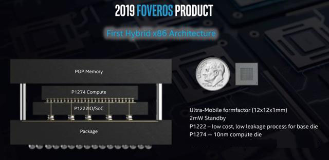
In the 3DIC field, Intel has launched Fovero technology, which adopts high-density bump(32um). Its greatly innovation is using active silicon carrier which uses high-performance logic chips stacked using advanced semiconductor processes are stacked on active silicon slides using mature semiconductor processes. The active silicon carrier itself is a chip that implements the IO interface circuit, and is expected to integrate other circuits suitable for mature processes (such as power management) in the future.
The fight between TSMC and Intel in the advanced packaging field
In the advanced packaging field, there is a competition between TSMC and Intel. In addition to the technical differences we have analyzed, the biggest difference between Intel and TSMC is the business ecology.
TSMC is the leading semiconductor foundry in the world. Its main business model is to help customers achieve success. So in the advanced packaging field, TSMC actively promotes opening ecology, including Packaging technology, interconnection interface standards, and associated IP, which hope to bring more values to customers. In future, as the price of the next semiconductor process becomes expensive, considering the cost, there are many companies choosing chip particles ecology. Therefore, TSMC's layout in recent years is obviously to create an opening ecology in the field of user cognition, technology and IP accumulation, thus continuing the previous success in the semiconductor industry.
Intel is the manufacturer of IDM. Traditionally, the process is mainly open to its own design and a few partners. In other words, its business model is not open. The advanced packaging technology is also opened to itself. Recently, as Intel’s process has lagged behind Samsung and TSMC, Intel’s processor has also surpassed by AMD, So Intel must depend on advanced packaging to reverse the situation. In addition, the traditional business——the growth of market of CPU is not stronger. Combined with several factors, the strategy of Intel depends on leading process to make powerful CPU and relies on CPU market to gain growth is not effective. Thus, one of methods for Intel is to depend on its accumulation of technology of advanced packaging to gain new growth. In order to realize advanced packaging technology, the best way is to adopt related ecology and open to customers to gain profits, this is the reason why Intel promotes chip particle ecology and opens its interconnection standard AIB. Recently, the architecture released by AgileX FPGA has directly encouraged users to inherit customized chip particles for user-customized systems. However, the chip particles technology needs supports from design and processing factory. If Intel wants to truly cultivate its chip particles ecology, it must further open its foundry business. At present, it seems that Intel's main way of opening up is still cooperative, that is, selectively cooperate with some design companies to develop chip particles design, which seems to be insufficient to truly cultivate the ecology. Besides, one point that needs to be addressed is the conflict between Intel's traditional CPU business and open advanced packaging technology—— semiconductor design companies want foundries to be neutral, however, Intel is unlikely to be neutral because it has a CPU business (for example, it will not open the process to AMD). If this contradiction is not handled well, Intel can only build around its own CPU/FPGA business and recruit some commercial ones. The ecology that allies join (like the previous AgileX system) is so destined to be big. At this point, TSMC has a natural advantage. Even if EMIB technology is currently leading in the cost, Foveros technology may not lag behind TSMC's SoIC technology, but Intel's business model and system are in conflict with the openness and neutrality of natural and ecological needs.
Related Articles:
Intel shows its brand new Sunny Cove architecture and 3D logic chip ...
OSAT has become a breakthrough of Chinese semiconductor industry
Huawei requests TSMC, the world's largest wafer foundry, to move a ...